Inside Nikon’s metal Additive Manufacturing strategy, Part 1: Hamid Zarringhalam on building a new growth pillar
Nikon believes metal Additive Manufacturing can become its next billion-dollar business. Backed by significant cumulative investment, the company is concentrating on defence, qualification strategy and production economics rather than general rapid expansion. Hamid Zarringhalam, in conversation with Martin McMahon and Nick Williams, explores how semiconductor-style process control and long equipment lifecycles underpin Nikon’s approach – and why execution, not enthusiasm, will determine how AM delivers durable industrial scale. [First published in Metal AM Vol. 12 No. 1, Spring 2026 | 20 minute read | View on Issuu | Download PDF]

Nikon has made clear its intention to establish Additive Manufacturing as a new pillar of growth. The measure of this ambition is not the declaration, but the substance behind it: is this corporate positioning, or a durable industrial commitment? Since our initial conversation with Hamid Zarringhalam – Corporate Vice President of Nikon Corporation and CEO of both Nikon Advanced Manufacturing Inc. and Nikon Ventures Corporation – at Formnext 2025, the company’s latest reporting has sharpened scrutiny of the economics of metal AM.
Nikon recently recognised impairment losses totalling ¥90.6 billion (about $608 million) in its Digital Manufacturing business, primarily through a write-down of goodwill and intangible assets associated with the Nikon SLM Solutions acquisition, and revised its full-year outlook accordingly. For the year ending March 31, 2026, it forecasts Digital Manufacturing revenue of ¥25 billion (about $168 million) and an operating loss of ¥105 billion (about $705 million) for the segment, including the one-time impairment charges [1]. This creates a more demanding financial backdrop for its long-horizon ‘pillar’ ambition and raises fresh questions about how Nikon plans to sustain investment amid a slower-than-expected adoption cycle.
When asked what the impairment does – and does not – change, Zarringhalam was unequivocal: “This does not, in any way, alter our market focus, customer strategy, or our unwavering commitments to our customers.” He added that Nikon’s view of the metal AM market “remains unchanged,” with particular focus on defence and space, “especially in the U.S. and Europe.”
This context matters because it shapes how he frames AM: less as a hype cycle and more as an industrialisation problem – process control, qualification and unit economics under uneven adoption. In Part 2 of our Nikon Advanced Manufacturing coverage in this issue of Metal AM, we report from Nikon’s Long Beach facility on how shared qualification and production support are being put in place.
Over a century in optics – now scaling metal AM
Zarringhalam uses Nikon’s origin story to frame how the company sees itself beyond the camera brand. “Before Nikon was even Nikon, Nikon started as a glass company, supplying glass to the Japanese military,” he said. “They made some scopes for the Japanese military during the war. But when it was over, there was no military, so they started to make lenses for photography.” From there, he explains, the business evolved over the decades from opto-mechatronics into semiconductor inspection and lithography systems.
Zarringhalam has spent thirty-eight years at Nikon, rising through the company’s precision and semiconductor equipment businesses. He describes being “deeply involved with the entire evolution of Moore’s law – and you know Moore’s law died several times along the way!” That is quite a career journey – enough to give just about anyone a claim to fame, given its significance for technological advancement and, in parallel, our development as a species.
Zarringhalam has built a substantial career across precision industries. Hearing him talk through Nikon’s lithography business, in particular, sheds light on why Nikon sees AM as adjacent to work it already does in high-precision systems. “So you print small things onto wafers for semiconductors. You print small things onto large glass for display. That’s all in the 2D world, but it is ultra-precise printing, it is total process control manufacturing, and it is also extreme quality-conscious inspection.” He added, “Then, we have metrology both within the machine itself as well as our standalone metrology company within Nikon’s Industrial Solutions unit.”
“So altogether now, the company is generating $4.7 billion per year in revenue. It’s about 40% in cameras and imaging, another third or so in Precision Equipment, which includes semiconductor and flat panel display lithography. Inspection and things like that are another $500 million, and we have $750 million in the healthcare business.” Nikon’s stated aim is to make Additive Manufacturing a pillar of growth, and in that context, Zarringhalam sees that pillar of growth translating into another close-to-billion-dollar business alongside what the company already generates elsewhere. Given the company’s history of success in precision equipment, it isn’t far-fetched to think Zarringhalam would add metal AM to Nikon’s story.
How Nikon built its AM position

Zarringhalam traces Nikon’s entry into AM back to a broader interest in digital manufacturing. “Digital manufacturing was the area that Nikon looked at, and broadly at that time, it was about how do you go from a CAD model into an assembled product?” In that context, he argues, metal AM felt adjacent to Nikon’s optics heritage: “Metal additive was a natural thing because that’s still light – that’s still driving and guiding that light into something.”
Directed Energy Deposition (DED) at Nikon originated as a skunkworks-style project – a small internal programme set up to move quickly. By 2020, Zarringhalam was asked to get involved. He recalled the broader strategy of not trying to do everything organically. As CEO of Nikon Ventures, he was well placed to pursue inorganic options, and Nikon’s first move was an investment in what was then Morf3D in El Segundo, California.
“My thought was, it’s a way to evaluate and learn more about this technology. Also, this was the area related to aerospace and defence, which we did not know enough about.” He explained that experience helped Nikon gain insight in the aerospace sector, understand the key players in the equipment market, and identify the main issues across the sector – and whether Nikon could help address them.
Like much of the industry at the time, Nikon concluded that Laser Beam Powder Bed Fusion (PBF-LB) had gained the most traction in metal AM, even if it was struggling to make significant strides beyond rapid prototyping applications. This led to Nikon’s acquisition of SLM Solutions. “We found good technology in a company that is synergistic with the values and the way we look at customers and technology innovation,” he said. “So we decided to acquire SLM Solutions.” The announcement surprised much of the market at the time.
Perhaps more significantly, the deal also marked the point at which Nikon’s cumulative investment in AM started to approach roughly $1 billion. As Lasermeister DED developed organically and Nikon acquired both a services business and a technology supplier, Nikon was committing at a scale it expected would reshape the business over the long term. “We modelled out what this business could look like, and decided that maybe in ten or fifteen years’ time, this is the next billion-dollar business.” The next pillar of growth.
Why Nikon believes metal AM’s success will come from defence
While the billion-dollar ambition remains intact, the path towards it has become more selective. Zarringhalam said AM accounts for about 3% of Nikon’s business; it’s understandable that reaching a billion-dollar scale will take time and sustained effort. He framed defence as the most practical route to near-term growth in metal AM. “Nikon Advanced Manufacturing has been steadily and consistently executing to a holistic strategic vision with focus on defence and space, and focus on the U.S. and Europe, and we expect those segments to continue to grow.”
“The underlying fact is that the total metal Additive Manufacturing market itself has not grown as quickly as predicted a few years ago due to slower AM adoption outside of defence and space markets, coupled with increased competition in those two segments, as well as bifurcation of the Chinese and non-Chinese markets.”
The U.S.
In the U.S., he argues, defence demand and policy priorities create a clearer pull for production adoption than many other sectors. Nikon, he added, does not want to operate as a service provider. Instead, it wants to be “a catalyst to accelerate the adoption of metal additive.”
That approach still required defence-specific know-how, and Nikon brought in retired U.S. Navy Admiral Michael Mullen in 2023 to advise on synthesising Nikon’s plans to focus on defence. Zarringhalam said Formnext 2025 may have been when he began discussing defence more openly in Europe, but argued Nikon had already been active in the sector for more than two years. “We’ve been very active in defence. I only started talking about it in Europe this year [2025]. But I was speaking actively about this in the U.S. prior to that, because in the U.S., defence was a big issue for understandable and expected reasons.”
U.S. defence demand is creating a stronger pull for faster, domestically anchored supply solutions, and this aligns with Nikon’s investment in its Long Beach centre. He described the site as set up to support large-format work and programmes where parts are difficult to source. “There have been shifts in timing and customer investment cycles while adoption in some areas has been slower than initially predicted,” he said. Even so, he argued that defence demand provides the strongest pull for near-term growth, and said the business would need to sustain roughly a 15% CAGR over the next five years to move toward its billion-dollar ambition.
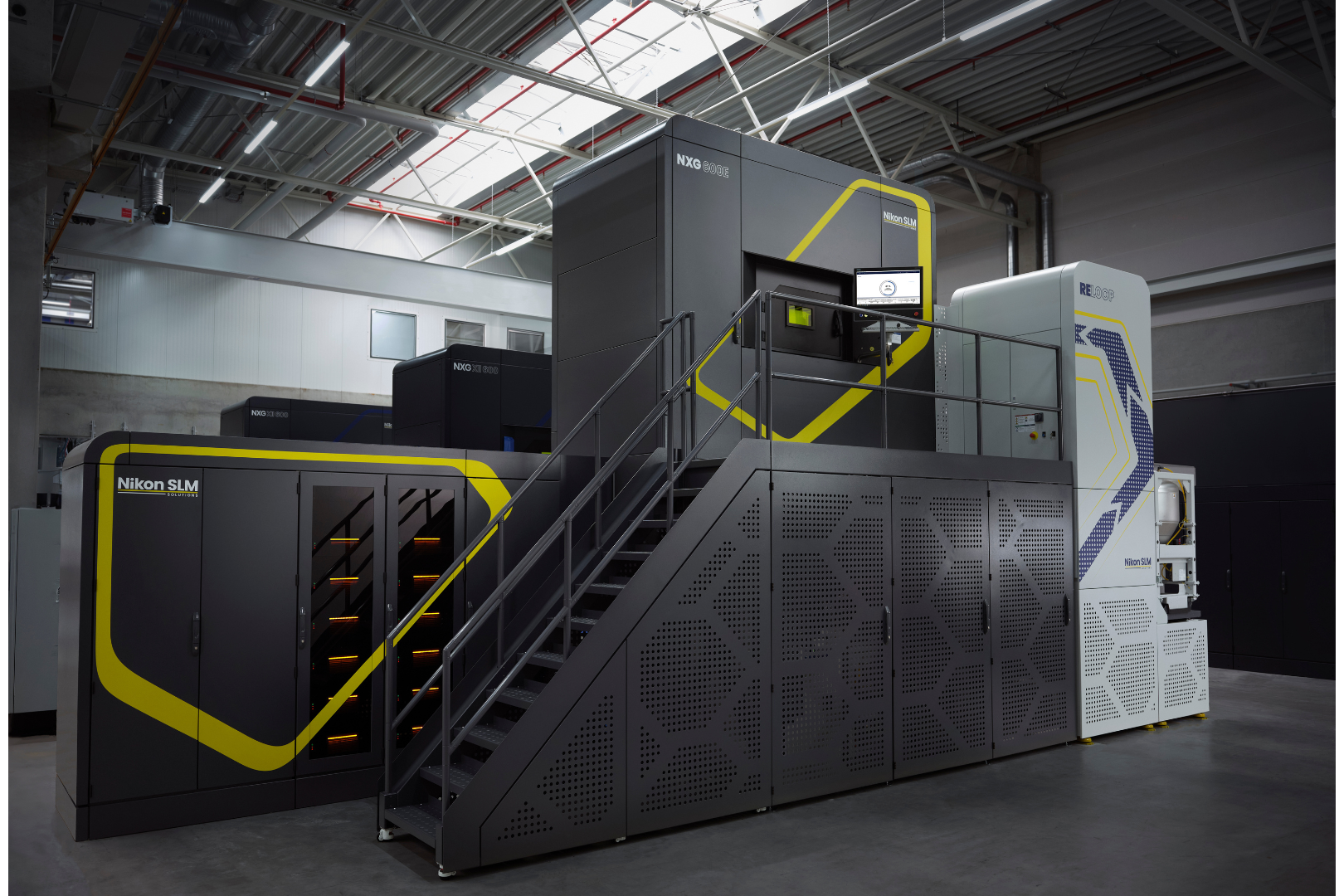
“I believe that probably the first two of the next five years will be moderate growth. Then ultimately, I think in the succeeding years, with a technology and business like ours (large platform NXG systems) that’s concentrating on defence, we are probably going to go faster than the general market.” He added that NXG machines already account for “about 60-65%” of revenues. He pointed to recent momentum on large platforms: “We have just recently closed additional NXG orders that validate our value proposition… for space applications with highly strategic customers.”
Interestingly, Nikon’s defence plans are not limited to large-format machines. The SLM®280 and SLM®500 remain part of the portfolio, including for customers outside defence, and Nikon does not plan to disrupt that installed base. For defence customers, he argued, the current portfolio allows Nikon to “meet their large format needs and all their medium-sized format needs.”
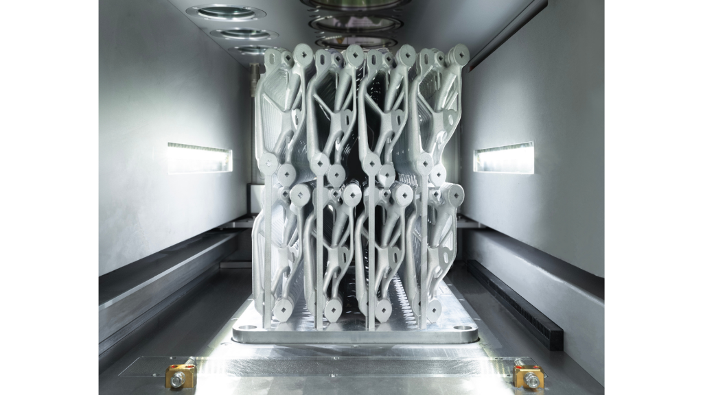
However, Zarringhalam hinted at further development. “We have a mid-sized machine platform capability today that’s public – there’s some stuff that’s not public – and so we think that market is important. We don’t stop at 600, right?”
Europe: slower path, less alignment
In Europe, Zarringhalam described a more fragmented environment – in procurement and in qualification approaches – including variation not only between countries but across defence bodies within individual nations. Nikon, he said, will focus on countries with the industrial capacity and political will to implement metal AM in defence. The practical implication is that faster progress in Europe will likely depend on greater alignment across qualification and procurement pathways. US programmes may still be imperfect, but they have generally shown more willingness to take controlled risk in building AM capability.
Japan: Indo-Pacific alignment and the home-market ‘bloc’ effect
Finally, Zarringhalam framed Nikon’s position as a Japan-headquartered company as relevant to Indo-Pacific defence priorities and allied manufacturing. “Indo-Pacific is such a big part of the U.S. defence strategy that a key pillar of that strategy is actually Japan,” he said. “Interoperability means we’re doing some manufacturing in the U.S., but we’ve got to be able to have that replication in allied countries, and Japan absolutely fits in.”
Using Patriot missiles as an example, he pointed to existing licenced production in Japan. “The Patriot missile is being manufactured in Japan by Mitsubishi Heavy Industries (MHI), under licence from Lockheed Martin,” he said. “So I see, whether it’s directly or whether it’s an offset programme, Japan will be picking up on defence, and AM will become a big part of it.”
Up to this point, Nikon’s near-term AM push may sound centred on US defence. But Zarringhalam also described Japan as a separate growth engine, where adoption can accelerate quickly once major manufacturers commit. In Japan, he suggested, when industry decides something matters, it tends to move together. Japan may be behind other industrialised markets in AM adoption, he said, despite Nikon’s global position. “We’re in a position where with our HQ in Japan, we are the biggest player in AM, but as of now, AM in Japan is pretty small.”
However, he also pointed to Japan’s heavy industrial base – including MHI, Kawasaki Heavy Industries (KHI) and IHI Corporation (IHI), and in automotive, Honda – and said these companies have been involved in AM for more than a decade. These mega-corporations operate across multiple sectors, meaning the net for AM can be cast very widely once evaluation phases are complete and they determine that AM is a strategic fit. Zarringhalam described the situation clearly: “Their R&D spans across several areas, aviation, auto, and much more, and we’ve got some big work that’s going on. I think when these things get validated, they will get propagated into other sectors. For instance, I see it extending to semiconductor, and that’s how Japan gets big.”
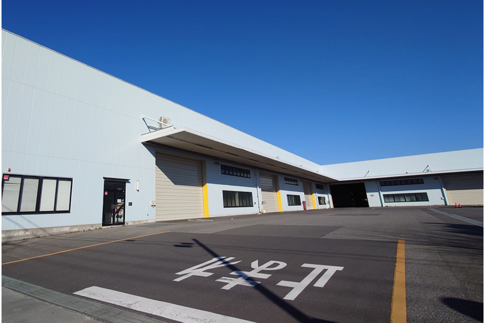
To support this, Nikon opened a new site in Gyoda, Saitama Prefecture, in February 2025, close to its semiconductor factory. The company has placed two NXG machines there alongside the Lasermeister LM300A and Nikon’s X-ray CT technology. “It’s probably not even one-third of the size of our Long Beach facility, but we’re doing some benchmark testing. We will probably do some parts for Japanese customers, demonstrations, and our part in the Japan Aerospace Exploration Agency (JAXA) project will be done over there.” He added that other parts of Nikon’s manufacturing businesses are likely to find uses for AM, and said several sites in Japan already have SLM®280s and SLM®500s installed. Simply from his thirty years in semiconductors, Zarringhalam said he hopes to see AM used there before too long.
China
When asked about the recent success of companies such as Apple in China, Zarringhalam described consumer electronics as a more cautionary market for Nikon. He knows the industry well and understands that the procurement culture in that sector is to drive everything to be “super-cheap.” Moreover, production in the consumer electronics sector is dominated by China’s domestic AM supply chain, so there is little rationale to pursue that market aggressively. He said, “For now, we are cautious about that sector.”

The bottlenecks to scaling metal AM
Qualification
“Advanced manufacturing often dies in qualification and testing,” Zarringhalam stated. The AM sector broadly recognises that one of the major barriers to the industrialisation of Additive Manufacturing is the gap between process qualification and part qualification, and Zarringhalam said Nikon sees the same challenge. He contrasted this with approaches that repeatedly qualify each material, feedstock supplier, machine, design and end-use application. Nikon SLM Solutions and Nikon AM Synergy, he said, are trying to do this differently.
Like others, the company first develops and validates parameters at the factory, which are transferable across all its machines. Because Nikon is specifically looking to serve the U.S. defence sector, Zarringhalam explained the company has been “closely partnering with both industry and government organisations in demonstrating Nikon Advanced Manufacturing’s abilities to deliver the necessary materials integrity, manufacturing quality assurance, and process control that are imperative for their most critical parts.” This work has included primes and specific branches of the U.S. military production infrastructure.
“The aim is simple,” explained Zarringhalam. “Generate the datasets once, validate collectively, and place them all into a central repository that the entire defence industrial base can use.” However, he admitted that this does not eliminate the burden of final part testing and said that it remains the major bottleneck. The difference, he argued, is that with a site like Long Beach, Nikon can stay involved. Customers are not taking the final qualification step alone; if something needs to be modified along the way, Nikon engineers are already working alongside them to address it.
From the conversations that followed during our visit to the Long Beach facility – covered in the companion feature – it was clear that Nikon is designing AM Synergy to support the kind of defence qualification work Zarringhalam alluded to. The site is set up for high-security programmes and for hosting shared qualification activities with customers and partners.

Economics: cost-per-kg and machine lifetime
It won’t all be about defence. Zarringhalam also pointed to space, automotive and energy as sectors Nikon has in view. In space, he said, there are already signs of growth, but he sees limits on the upside – particularly as the industry pushes toward re-using hardware. Space activity remains largely US-led, followed by Europe, and specifically relevant to Nikon, Japan is also increasing spending through the JAXA programme. “It’s not going to be a repeat of SpaceX,” he said, “but it is going to be big, and we’re already a part of it.”
Automotive is highly cost-sensitive; on a cost-per-kg basis, more so than aerospace. In his view, adoption will expand as the cost of AM production declines, driven by improvements in AM machines, materials, and energy efficiency. He added that wider adoption also depends on confidence in the equipment’s lifespan and reliability, with machines expected to perform for at least ten years – and ideally longer.
More broadly, Zarringhalam framed AM adoption as an economic problem driven by availability, throughput and yield – a problem that can be addressed through laser count and power, and through data movement, ease of use and maintenance strategies. He said Nikon is less focused on headline claims and more focused on meeting cost-per-kg requirements that can support sustained production. That’s why Zarringhalam pushed back when asked about the market’s perception that machines become obsolete after just three years. “I’m going to go back to semiconductor. We have machines in the industry that people have been using for thirty years, and what’s nice about that is, after five years, that machine is completely depreciated.”
Nikon’s AM portfolio
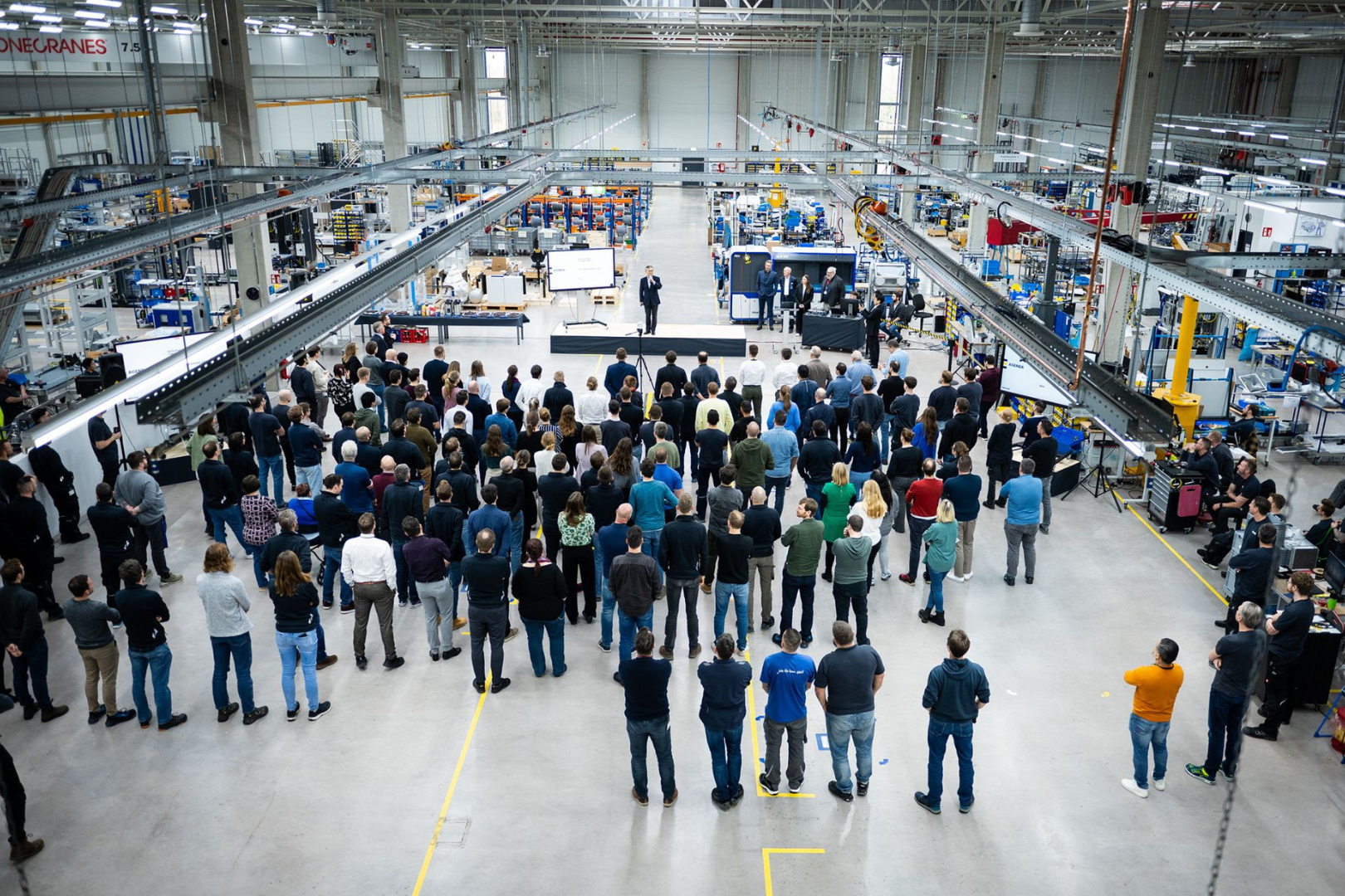
We’ve seen that, other than the self-developed DED business, Nikon has taken the bold step of acquiring AM market share through strategic acquisitions. But what does the pedigree of ultra-precision optical systems mean for the existing SLM technology?
“You have to remember that the technology is inherently old – not very old – but you’ve got some limitations on what you can do,” Zarringhalam said, gesturing toward the NXG mock-up outside. “That’s why the other stuff that we’re working on allows you to really unlock new capabilities, and do a whole lot of new stuff.” He added that within PBF-LB, Nikon is advancing the SLM®280 and SLM®500 for sectors such as medical, where certification is demanding and performance and reliability are central – a theme explored in greater detail in our companion report from Long Beach.
Financial realism behind Nikon’s long game
For all the ambition, Zarringhalam was direct about return expectations. “Today, if you look at our financials, our business actually is losing money,” he said. “No company can withstand that unless you have a diversified business, unless you have a long-term view on where this has a pillar of growth.”
He also stressed that growth is not linear – particularly for a company with Nikon’s history – and described the path as inherently uneven. The point, he said, is having the resilience and governance to keep investing through those periods.
He mentioned in a pre-Formnext event that reinvestment into R&D was running at around 20%, and I asked how long that could be sustained. Zarringhalam said that, in percentage terms, this would change as revenues rise – even if absolute R&D spending increases. He also said work currently in development would come to market and support revenue growth. Ultimately, he framed it as an obligation to deliver for shareholders: that is, he has to make AM a billion-dollar business over the long run.
Zarringhalam’s tone was notably unhyped, shaped by decades in semiconductors and experience living through repeated cycles of Moore’s Law expectations. He described Nikon’s AM business as loss-making today and acknowledged that part qualification remains the principal bottleneck to wider industrialisation.
At the same time, the commitments are tangible: roughly $1 billion of cumulative investment, the build-out of Long Beach, concentration on large-format NXG platforms, and a pooled-data approach designed to reduce duplicated materials qualification across the U.S. defence industrial base. The strategy is clear. Rather than wait for broad-based adoption, Nikon is concentrating capital and organisational focus where urgency, policy alignment and programme funding are most likely to convert capability into production revenue.
That concentration carries risk. Defence-led growth narrows exposure and ties momentum to procurement cycles and geopolitical priorities. But it also imposes discipline. Nikon is effectively applying semiconductor capital-equipment logic to metal Additive Manufacturing: long machine lifetimes, controlled process environments, shared validation frameworks and scale built over decades, not refresh cycles.
Whether AM becomes a durable new pillar for Nikon will depend less on headline machine performance and more on execution – on qualification throughput, cost-per-kg economics and the company’s ability to sustain investment through good and bad years. If those elements hold, Nikon’s bet is not on hype-driven expansion, but on industrial necessity gradually turning into repeatable production demand.
Author
Martin McMahon
Technical Consultant, Metal AM
Founder of M A M Solutions
Further information
https://ngpd.nikon.com/en/material-processing
https://nikon-slm-solutions.com
References
[1] Metal AM, ‘Nikon reports lower metal AM revenue, revises outlook for 2026’, February 9, 2026, available at: www.metal-am.com/nikon-reports-lower-metal-am-revenue-revises-outlook-for-2026/

LAST MONTH’S MOST-READ ARTICLES