

High-performance product development in the era of computational design: A case study with nTop and NASA
The era of computational design is reshaping the engineering and product development landscape, enabling industries to tackle complex design challenges with unprecedented speed and efficiency. This article explores how NASA, using software from nTop, leveraged cutting-edge tools and methodologies in a unique application development. In combination with the capabilities of Additive Manufacturing, the project saw a scientific instrument component’s original material, beryllium, replaced with an aluminium alloy, providing a significant part cost reduction whilst exceeding all necessary performance requirements. [First published in Metal AM Vol. 10 No. 4, Winter 2024 | 10 minute read | View on Issuu | Download PDF]
Driven by advances in computing power, Artificial Intelligence, Machine Learning, and digital manufacturing, the era of computational design has arrived – and it is poised to make an even bigger impact than any previous era of design, from paper to Computer Aided Design (CAD) to parametrics.
More to the point, computational design is quickly transforming how design-intensive industries solve complex problems in engineering and product development. These industries share similar goals: deliver high-performance products on faster timelines. Increased performance might mean faster aircraft, improved osseointegrative medical implants, cost-effective automotive vehicles, more sustainable consumer products, or the decarbonisation of the global industrial ecosystem. In all these cases, computational design is breaking down the barriers of conventional design tools.
The primary issue with conventional tools is the speed of iteration. Constrained by manual modelling of low-level design features, defining complex relationships between design features that are difficult to construct, and complex real-world physics, these tools simply move too slowly to support a highly iterative process required in high-performance product development.
Computational design solves this problem with algorithms that capture design intent and logic in order to generate solutions to complex engineering problems. When this happens, computational design effectively provides engineers with solutions to generate, visualise, explore and evaluate vast design spaces more rapidly. Ultimately this leads to better, more informed decisions and optimal solutions.
Importantly, a computational design model doesn’t just capture one version of a design. Since it evaluates intent and requirements algorithmically, the model effectively calculates an entire design space that represents the complete scope of what is possible. This key difference enables a massive improvement in the speed of iteration. The building phase of a model might take a bit longer than drawing it manually, but once it is built, engineers can iterate in rapid-fire fashion.
Furthermore, significantly faster iteration empowers engineers to optimise products and incorporate manufacturability earlier into the process. This means engineers can find better solutions that balance production economics and quality and dramatically reduce time to market. The fact that design intent is ‘baked in,’ means that computational models can be version-controlled, reusable, and extensible to solve similar design problems.
What does that look like in actual practice? In a recent instance with Siemens Energy, the differences were stark: iterations were completed in seconds and minutes rather than hours and days. Using rapid iteration, the design team ran two hundred designs with just twenty-three errors – a success rate close to 90%. With traditional boundary representations (B-rep) CAD tools, the expected success rate is closer to 30%. In addition, design files that would have been 200 MB with traditional tools were just 3 MB.
All mainstream CAD systems use boundary representations (B-reps) as their geometric modelling technology. As the name implies, a B-rep describes a shape by modelling its boundary. The part’s skin is wrapped in a collection of faces joined at the edges.
Computational design requires five key capabilities
To realise these benefits, computational design requires models that can respond intelligently to parameter changes – regardless of whether those changes are initiated by an engineer or a powerful computing platform. Specifically, these models must be:
- Fast
Faster iteration demands features such as automation and real-time model updates that enable engineers to visually assess design changes more rapidly. - Flexible
Models require a high degree of freedom to change in order to capture a large design space. They need to support broad changes in shape, topology, material distribution and composition. - Reliable
Computational design relies on modifying inputs and recomputing the model, so computations must be reliable or the model will fail to update. - Closed loop
For a computational model to be useful for engineers, the physics must be fully integrated in order to facilitate closed-loop optimisation. Results from a structural analysis, for example, may indicate the stress value at each point in a design. These values form a scalar field that triggers automatic modifications that add material to strengthen areas of high stress and remove unnecessary material from low-stress areas. - Differentiable
A common design objective is to minimise a design property, such as manufacturing cost or weight. To find a minimum, the engineer (or computer) needs to know which direction is ‘downhill.’ This requires mathematical differentiation, because derivatives indicate how parametric changes will affect the design and which changes will improve it.
The power of implicit modelling
The primary difference between computational design and traditional CAD tools is seen in how they represent geometry. B-reps have significant flaws that make them unsuitable for computational design. In fact, their architecture has remained mostly unchanged for decades. As a result, they are not suited to parallel computing, especially GPUs.
In a typical B-rep system the GPU renders triangles from a geometry kernel running single-threaded on one core of a CPU. B-reps are also unreliable and calculations fail for a variety of reasons, despite significant efforts to make them more resilient over the past four decades.
Computational design uses a completely different approach called implicit modelling. With implicit modelling, the shape of an object is described by a mathematical function that returns the distance to the closest point on its surface. The function is constructed so that it will be negative inside the object, positive outside the object, and zero on the surface. This is why it is called a Signed Distance Function (SDF).
This is critical because a key step in any modelling algorithm is deciding whether a given point P is inside or outside an object. If you have an SDF, this is easy: you simply check the sign of the function of P. This calculation is easy to parallelise because the results for different points are independent of each other. For this reason, implicit modelling calculations are incredibly fast on GPUs, delivering real-time interaction even for the most complex, intricate shapes.

How NASA uses computational design to replace beryllium with aluminium
The best way to understand the power and potential of computation design is through real-world examples of product development teams focused on high-performance products in competitive and demanding industries.
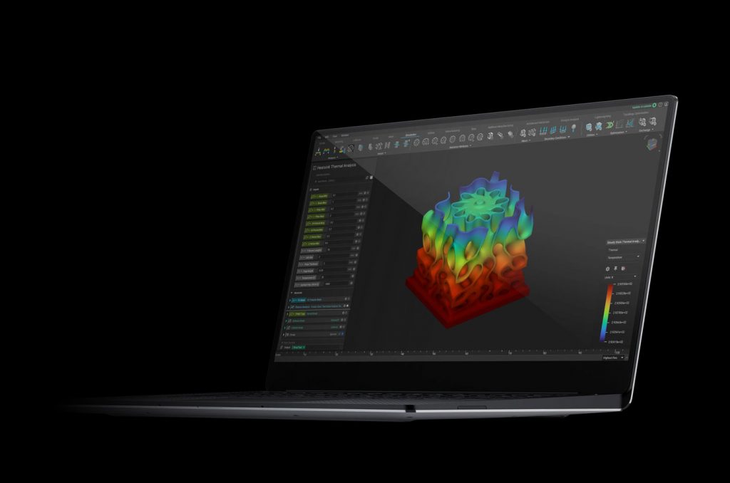
In this case, engineering research conducted at NASA Goddard Space Flight Center in Greenbelt, Maryland, was focused on the baseplate of a laser benchtop system. As the laser transmits heat to the baseplate – 200 W in the centre, running continuously – the surface deforms, compromising the accuracy of measurements taken with the laser. This design challenge is relevant to a wide range of laser, LiDAR and photonics systems used in aerospace.
Today, these baseplates are made from beryllium, a material that is extremely stiff and resistant to deformation under thermal loading. Unfortunately, beryllium is also very expensive and its dust is extremely toxic. There are also only a limited number of shops qualified to machine beryllium for aerospace applications, so lead times are very long.
The NASA team sought to replace beryllium with a safer, less expensive material without compromising performance. The chosen material was A6061-RAM2, a general-purpose AM aluminium alloy with an elastic modulus of less than half of beryllium. There is essentially no way to do this without computational design – an approach that can produce and optimise lattice networks engineered to enhance specific characteristics, such as strength and heat transfer.
In particular, the team wanted to determine a lattice network that could achieve similar deformation performance of forged beryllium with: an equivalent elastic strain (Von Mises strain) similar to beryllium, an equivalent stress (Von Mises stress) less than beryllium, and mass targets within ±10% of beryllium.
“You’re taking a cheaper and relatively weak material and asking how to make it outperform an extremely expensive advanced material that’s 33% lighter,” stated Alex Souk, a Senior Mechanical Design Engineer at Goddard who helped lead the project. “You have five constraints and it’s a multi-physics problem. This is really difficult to solve.”
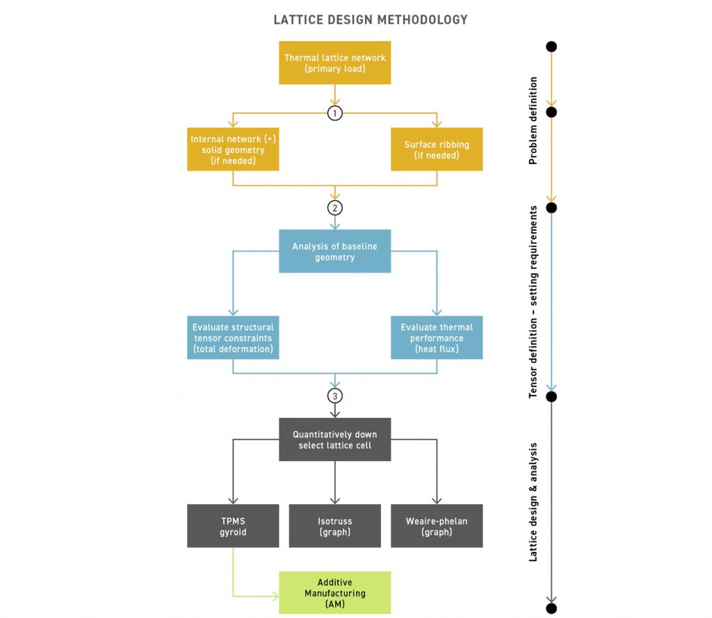
Developing a systematic approach to lattice design
Computational design held the key to the NASA team’s approach. The team was particularly interested in constructing a systematised lattice design methodology that could be shared and reused in many other applications across NASA (Fig. 3).
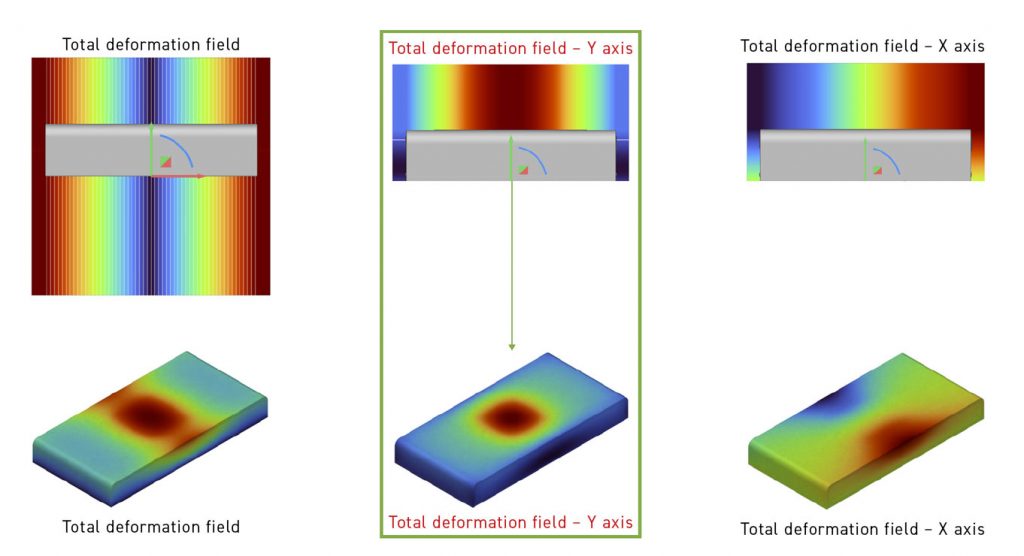
The team started by establishing the vector field for optimisation. This involved simulating the thermal stress of the laser on both materials. As the team expected, the beryllium plate performed well with very little deformation (1.56E-5), and the aluminium performed poorly with significantly more deformation (4.43E-5) (Fig. 4).
This field was imported into nTop software where a ramping function was applied. This capability lets engineers gradually change a value based on the scalar field. For example, areas of the part that experience high stress can be thickened while low stress areas remain as is.
“Due to the way nTop generates the geometry, you can specify that in areas where deformation exceeds a certain threshold, a certain thickness is needed,” Souk explained. “Then we can ramp it back down by the time it gets to low deformation. nTop varies the scale of design parameters based on actual simulation data.”
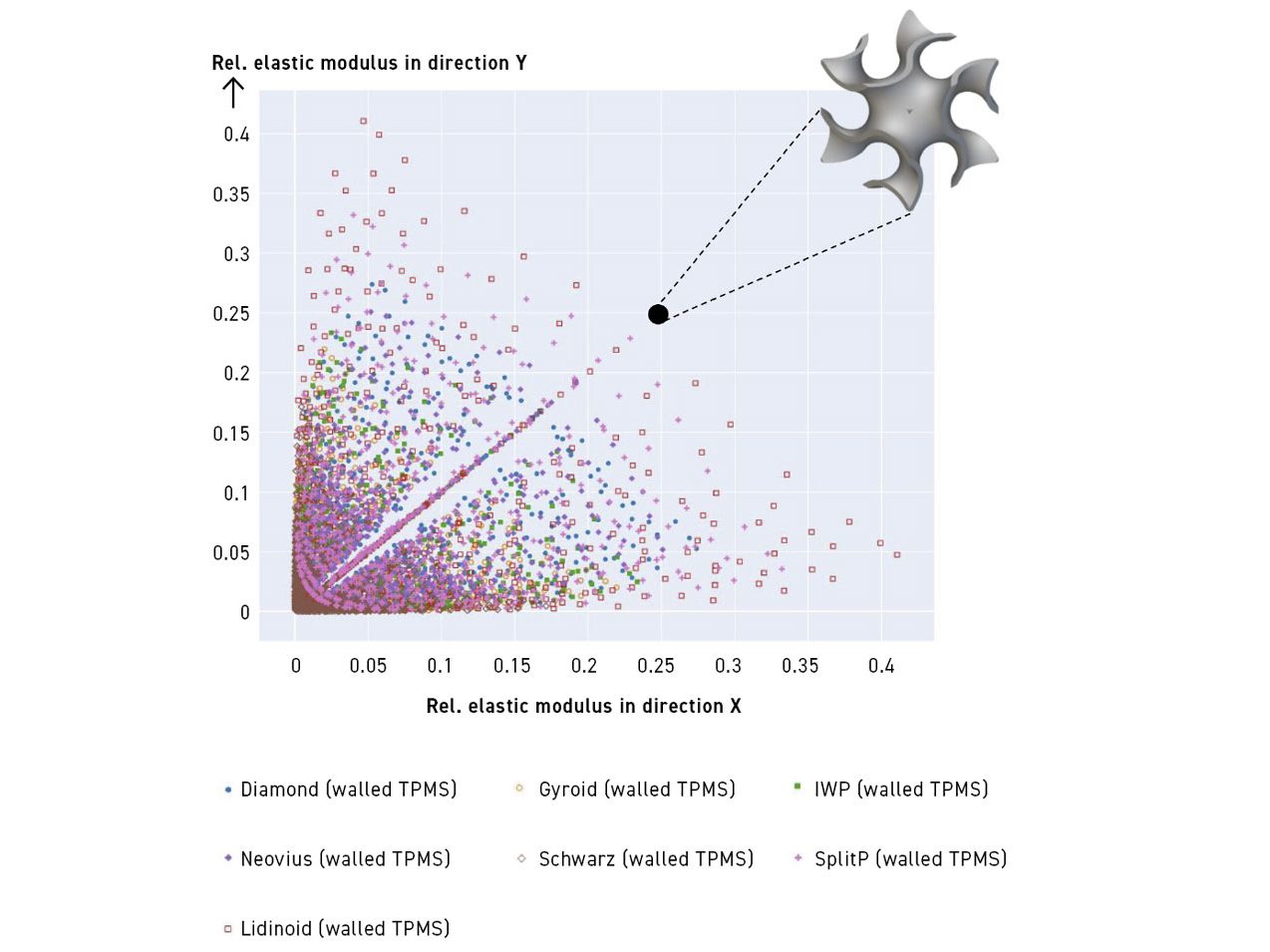
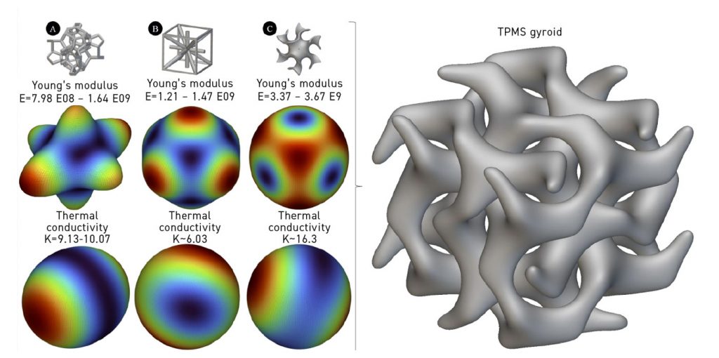
From this point, the team needed to figure out which lattice network to use, which is a perpetual problem in latticing. The team used a three-body diagram to understand the relevant physics models and then normalised the data to quantify the data of interest. Some lattices are stronger in certain directions, and other lattices are better for conduction. This quantifiable down-selection process led the team to consider three candidates based on the elastic modulus in the Y direction: a TPMS gyroid, an isotruss and a Weaire-Phelan structure.
In collaboration with Dr Ryan Watkins at NASA’s Jet Propulsion Laboratory in Southern California, the team performed homogenisation to characterise equivalent material properties of different lattice unit cells. This revealed that the TPMS gyroid had the highest resistance to deformation (based on Young’s Modulus) and the highest thermal conductivity (Fig. 6). In addition, it would be easier to manufacture than the others.
“The next step was determining the structure, which we believed would include Voronoi ribbing at the top layer to keep the skin strong, a gyroid-based lattice core that will do most of the heavy lifting, and then an aluminium wrap around the whole thing,” Souk stated. “Then we got to work simulating all the different configurations to identify the optimal solution” (Fig. 7).
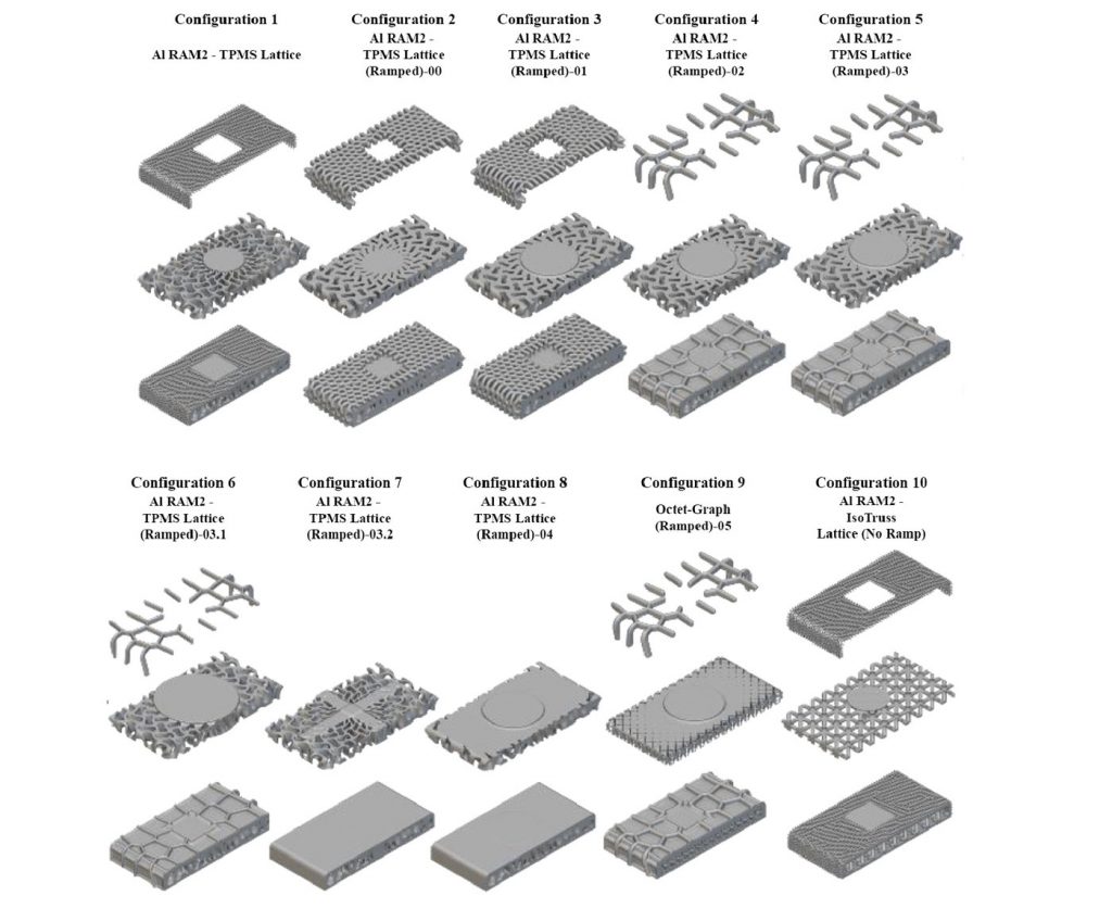
With nTop, the team was able to determine how the Voronoi ribbing impacted performance at a specific mass penalty. This helped them quickly iterate on a variety of configurations of ribbing structures and lattice networks. With these configurations established, the team performed a design of experiments (DOE) to find the most successful one.
“We ramped up certain values and looked at the results, looking at the convergence of data in physical properties and manufacturability,” Souk stated. “We tried a lot of options with respect to thickness, dimension, Voronoi ribbing, and internal various internal lattice structure. You see what works and what doesn’t and then adjust for a new iteration.” Each iteration takes approximately five minutes to develop, but then it has to be simulated in a separate ANSYS software platform.
“Using nTop you can build workflows intelligently knowing what variables you intend to change,” Souk added. “Then you can copy it, change those variables, and the model updates parametrically. We validated results in ANSYS, which is widely used in the industry.”

Meeting stringent requirements for all five constraints
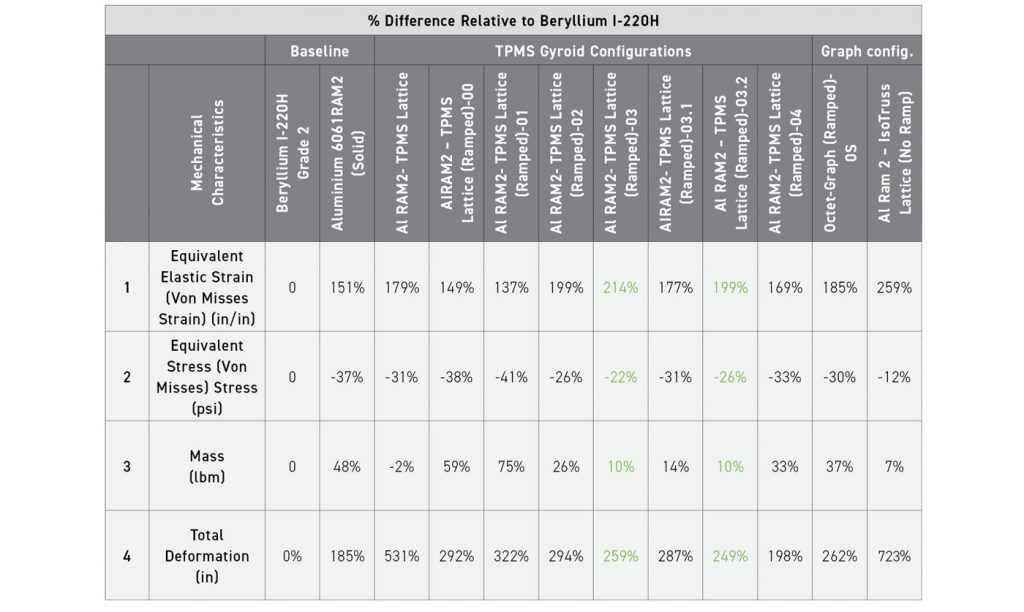
The results of the DOE were extremely successful. The winning AM aluminium model delivered a 10% mass penalty compared to beryllium but 22% less internal stress. Its deformation was 259% more than beryllium, but this percentage is less important than the actual difference in deformation due to the micron-level scale of the application.
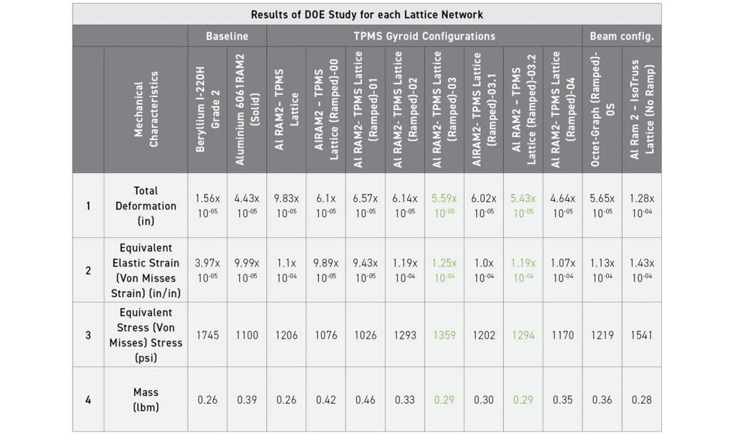
“With this particular TPMS lattice, the difference between the two materials needs to be within 5 µm ± 10%,” Souk stated. “We knew the aluminium would deform more than the beryllium. The question is, did we hit our requirement? In our case, the answer is yes.”
Specifically, the deformation with the beryllium baseplate was 0.396 µm while the deformation with the AM aluminium baseplate was 1.419 µm. This means the total average deformation difference between the two materials was ~1 µm (±10%).
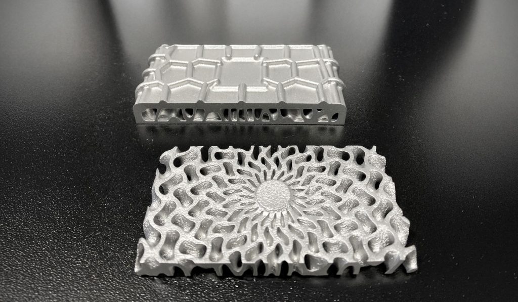
Importantly, the AM aluminium model delivered two other benefits in terms of its cost and fabrication time. “The configuration we chose has the gyroid lattice core with the Voronoi at the top, and they print really well,” Souk stated. “We were able to define the features of the lattice without any issues, with clear separation in strut thickness between the two boundary layers. The final part was fabricated at NASA’s Wallops Fliht Facility in Virginia in nine days at a total cost of $1,200.”
Compare those numbers to the beryllium part, which requires a thirty-six-week lead time and costs $20,000. “Ultimately, we were able to construct a lattice, optimise it, reduce our lead time by 36x and our cost by 20x,” Souk stated. “The aluminium part outperformed beryllium in terms of internal stress with an acceptable mass penalty and within a micron of performance. That’s a huge win for latticing.
“The fact that AM aluminium macroscopic mechanical meta-materials can compete with materials like beryllium could have significant follow-on effects at NASA.
“The applications for this have exploded. We have created a new unit cell that outperforms wrought aluminium for avionic packaging. There is another candidate in process for structural acoustics. Macroscopic mechanical metamaterials and nTop are also assisting in exciting research in the space of multi-material manufacturing under Russel Stein at NASA GSFC Code 543: Mechanical Systems Division,” Souk explained.
“We’ve been using nTop for a little over a year and we’re already submitting to a scientific journal, we have pre-patent applications, and a part that is currently being qualified for flight on a spacecraft,” Souk concluded.
Author
Evan Pilz
Senior Application Engineer
nTop
[email protected]
www.ntop.com

LAST MONTH’S MOST-READ ARTICLES