

International Conference on Electron Beam Additive Manufacturing: Highlights from EBAM 2023
Since the first conference on electron beam Additive Manufacturing in Nuremberg in 2016, the EBAM conference series has been the central meeting point for industry and academia to exchange knowledge on this dynamic area of AM. After the event was forced to go virtual in 2020 due to COVID-19, attendees were finally able to meet face-to-face again in Erlangen, March 22-24. Marie Franke-Jurisch and Dr Matthias Markl report on recent developments in materials, process, and machine technology, all of which serve to demonstrate that electron beam-based technologies are once again firmly established in the metal Additive Manufacturing world. [First published in Metal AM Vol. 9 No. 2, Summer 2023 | 20 minute read | View on Issuu | Download PDF]

The EBAM conference series was launched in 2016 by Prof Carolin Körner and Dr Matthias Markl from Friedrich-Alexander-Universität Erlangen-Nürnberg (FAU) to address technological and process-related hurdles and challenges in the field of electron beam-based (EB) Additive Manufacturing. The goal was to bring all experts in the field together to accelerate developments in both research and industry. The presentations covered the complete process chain, from powder production and reuse to the post-processing of components. From a materials perspective, the focus was on the processing of titanium alloys, steels, and nickel-base alloys. Additionally, process monitoring approaches, modelling and simulation were featured with a view to contributing to a better understanding of physical effects during the build process.
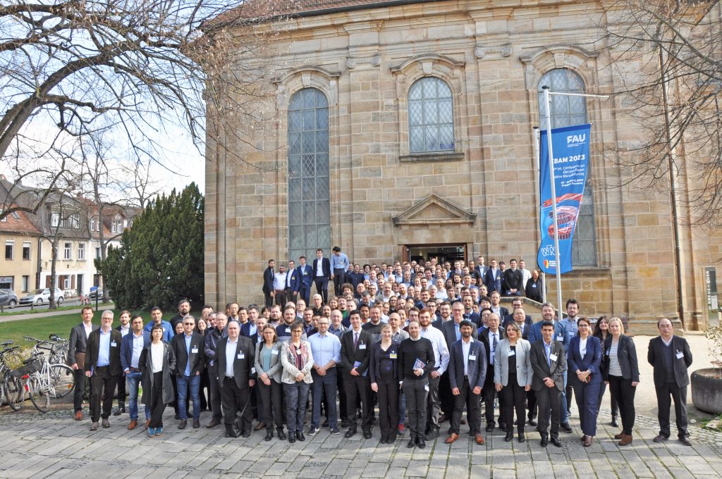
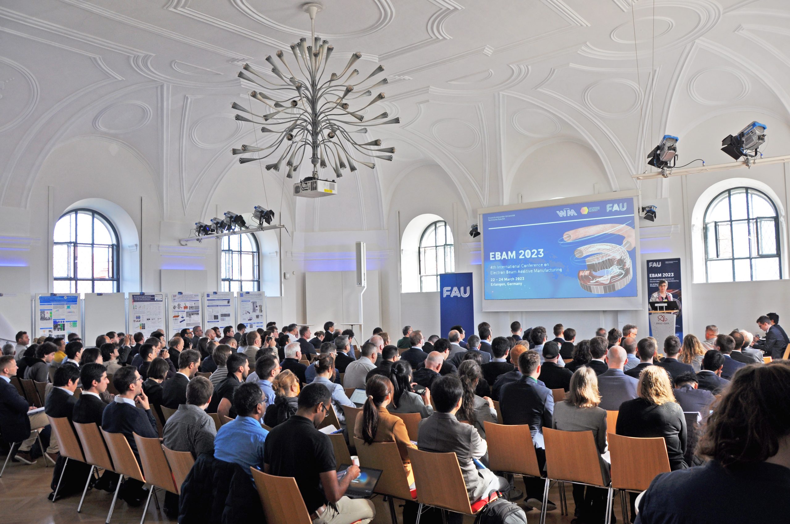
This successful conference format remained unchanged for this year’s fourth edition of the conference, held in Erlangen, Germany, from March 22-24, and attracted the interest of a broad international community with participants from seventeen countries.

Since well before 2016, electron beam-based technologies had already gained a foothold in a wide range of industrial sectors. This was reflected well in the focus of the presentations as well as in the number of participants at this year’s event. Noticeably, process-related variability and the monitoring of reproducible and optimised materials properties and microstructures are coming to the fore among topics. This is being driven by advances in simulation-supported alloy design, process simulation, and, above all, by software and AM machine innovations that increase both the degrees of freedom in scientific development and the feasibility in industry of both Electron Beam Powder Bed Fusion (PBF-EB) and wire-based Electron Beam Directed Energy Deposition (DED-EB). While these topics were the subject of numerous virtual poster contributions in Nuremberg in 2020, their ongoing development was explored in greater depth in several presentations in Erlangen. For the first time, this year’s conference was also accompanied by a small exhibition.
The following review presents some highlights from EBAM 2023 covering process development, new machine concepts, alloy development, scan path optimisation, process monitoring, powder production, and material processing.
Areas of focus for PBF-EB research
The fact that the combination of the previously discussed research and development approaches are the basis for the complex processing of materials was made clear by Prof Andrey V Koptyug from the SportsTech Research Centre at MidSweden University, who gave the opening lecture at EBAM 2023 [1].
At the beginning of his presentation, the main research areas in the field of PBF-EB were summarised. According to Koptyug, materials and powders, as well as machine technology, in-process control and simulation techniques, influence the success and efficiency of the process chain. In combination with post-processing, these issues have a significant impact on the quality of the final components and provide insight into the great potential of the technology.
While the importance of these topics was barely recognised in the shadowy early days of all metal-based AM technologies, the PBF-EB process is now experiencing a significant boost in public interest. Koptyug illustrated this with a simple random search on ScienceDirect, which gives an idea of the historical development of scientific publications on the PBF-EB process (Fig. 3).
![Fig. 3 A quick search in ScienceDirect database including covers, research papers, books, and book chapters among the two categories of “Find articles with these terms” and “Title, abstract, keywords” for the terms “Electron beam melting”, “Selective Electron Beam Melting”, “Electron Beam + Powder bed” [1]](http://www.metal-am.com/wp-content/uploads/sites/4/2023/07/fig-03-5-1024x419.jpg)
Furthermore, he reported on a major existing bottleneck of the technology: powder removal from porous or lattice structures. PBF-EB medical implants rely on a level of surface porosity to enable osseointegration (bone ingrowth into the surface of the implant), but the technology is also used in other functions such as lightweight construction, energy absorption, or the tailoring of physical properties.
In a study, the team investigated the influence of different post-processing approaches for powder removal from lattice structures. Here, they compared the standard solution, the powder recovery blast system (PRS), with ultrasound vibration-assisted powder removal and chemical etching. While powder remained in the grid with increasing density when the PRS was used, subsequent etching did not result in further powder removal. It also affects the mechanical properties by removing surface layers and, consequently, changing the cell geometry. In contrast, the ultrasonic vibration method proved effective for powder removal after using PRS. However, very fine lattice walls were damaged. It is also interesting to note a potential effect on the microstructure, as these workers reported a fine-grained structure as a result of the vibrations [2].

In addition, Koptyug considered materials development as an important branch of PBF-EB research. Here, he shared insights into the in-situ alloying of powder mixtures, which can be used advantageously in PBF-EB due to its increased build temperatures, among other things. He investigated the microstructures and properties from a Ti-Nb powder blend using scanning electron microscopy (SEM), electron backscatter diffraction (EBSD) measurements, and nano-hardness indentations.
Koptyug emphasised the difficulty of microstructural homogeneity, which is strongly dependent on individual melting points, among other factors. If the difference is too great, this can lead to inhomogeneities, for example, due to non-melted areas and local material vaporisation, or contribute to the formation of viscous melts that make processability difficult. On the other hand, the powder blending approach enables the development of high-cost materials such as high entropy alloys, shown here on an Al0.5Cr1.0Mo1.0Nb1.0Ta0.5 alloy, or magnetic materials such as AlMn(C) or metal matrix composites (MMC) using the example of a powder blend of gas atomised 316L and WC. He also postulated the potential for functional graded materials and bulk metallic glasses.
Finally, as a highlight, he reported on the integration of an additional infrared source into the machine for temperature adjustment. Fig. 4 shows promising results, which make it possible to reduce layer times, save energy, reduce filament damage, avoid so-called ‘smoke events’ and even build without a start plate.
![Fig. 4 Left: Bottom temperature during the first forty layers using NIR- (near-infrared) and conventional EB-preheating, Right: EB-built structures using NIR-technology for preheating. [1], reprinted from [3] under a CC BY 4.0 license](http://www.metal-am.com/wp-content/uploads/sites/4/2023/07/fig-04-4-1024x509.jpg)
According to Koptyug, the aforementioned capabilities offered by PBF-EB lead to spatial control of properties, thus opening what was described as a ‘fourth dimension’ in Additive Manufacturing.
New PBF-EB machine concepts
In contrast to previous conferences, EBAM2023 had seven AM machine manufacturers present: Freemelt, GE, ALD, Wayland, Pro-Beam, JEOL, and QuickBeam Technology.
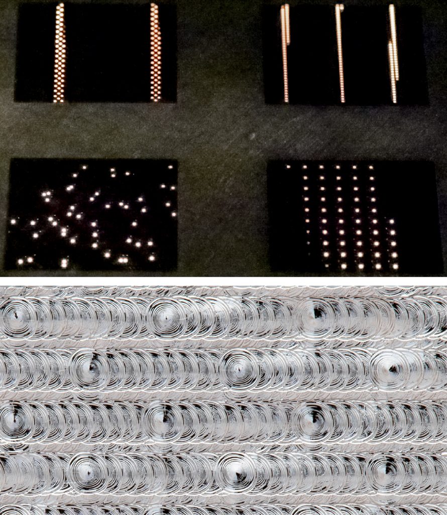
In his presentation [4], Ulf Ackelid, principal scientist and co-founder of Freemelt, Sweden, referred to the open structure of the company’s software, Pixelmelt, and addressed an emerging topic in the PBF-EB world – beam scanning patterns – which also found resonance in other presentations, including those by Christoph Breuning [5] and Paria Karimi [6].
Software provides easy access to previously script-based scanning strategies. According to Ackelid, the electron beam can jump between tens of thousands of melting points per second, enabling a balanced distribution of heat. Developments around this topic help to understand the thermal history of a material as a result of its melting and allow us to modify it so that a material’s structure – and thus its mechanical and physical properties – can be targeted, even within a component.
It was stated that melting powder layers in discrete spot patterns is particularly beneficial in Freemelt’s PBF-EB technology because of the consistent e-beam spot quality over the whole power range up to 6 kV in Freemelt’s diode electron gun. Spot melting at very high beam power will lead to higher productivity, according to Ackelid. This is demonstrated in Fig. 5 by various spot melt patterns and a resulting tungsten-based melt surface [4].
It was not just on the machine software side that innovations were announced. Martyn Hussey from Wayland Additive, UK, presented a way to avoid smoke events by using the so-called ‘NeuBeam’ technology [7]. When the electron beam strikes the powder, the charge cannot be dissipated due to the low conductivity of the loose particles, causing the powder particles to become electrically charged. In the Wayland process, the particles can reach potentials up to the level of the incident beam (e.g. 60 kV), Hussey stated.
Due to the Coulomb repulsion of the negatively charged particles to each other, a smoke event can occur. Instead of the known solution of setting a low conductivity by slightly sintering the powder bed, the charges of the particles are neutralised using NeuBeam technology. This is done by an initial flooding of the powder bed with positively charged Ar ions before starting the electron beam. Charge neutralisation follows, while energy is delivered freely to the powder bed.
According to Hussey, this technique is already established in other industries, such as X-ray photoelectron spectroscopy and Auger electron spectroscopy, and it has now been transferred to the Calibur3 machine. Another advantage is that the powder bed no longer needs to be sintered, which should have a positive effect on the flowability of the powder cake and, thus, on powder removal in internal structures, as Fig. 6 shows.
![Fig. 6 Active charge neutralisation (top) and the sinter-free depowdering of a lattice structure (bottom) [7]](http://www.metal-am.com/wp-content/uploads/sites/4/2023/07/fig-06-2-882x1024.jpg)
The smoke issue was also approached by other equipment manufacturers and in further scientific contributions such as the NIR technology described at the beginning [1]. For example, Camilo Medina Viramontes from Freemelt, Sweden, also reported in his poster on the development of the ProHeat® technology [8], in which the powder bed is already slightly sintered from above via infrared radiation to eliminate the propensity to smoke.
Viramontes claims that this patented technology will expand the range of processable alloys for PBF-EB. Using ProHeat, all types of powders can be pre-sintered without the risk of smoke, regardless of powder size and electrical conductivity. Furthermore, Ralf Edinger from Canmora Tech, Canada, reported on ball milling as a method of reducing charges in the powder bed [9]. He showed that it could be used to process steel powder smoke-free at room temperature. Finally, Dongfang Wang [10], from Tsinghua University, China, also spoke about the earliest possible detection of the initiation of a smoke event and its possible prevention.
Another highlight from the series of equipment-related innovations was the presentation of the PB EBM 30S machine concept by Sebastian Pohl [11] from pro-beam additive, Germany. The technology is distinguished by its high beam energies of up to 15 kW. For practicable implementation in existing production environments, the BuildUnits as well as a transport unit help to simplify the powder handling problems to a large extent. Pohl also reports that by using several BuildUnits, both the build process and the relatively slow requirement for cooling under vacuum conditions, can run in parallel. This leads to a further increase in productivity (Fig. 7).
![Fig. 7 The parallelisation of process steps at pro-beam [11]](http://www.metal-am.com/wp-content/uploads/sites/4/2023/07/fig-07-2-1024x470.jpg)
Fuad Osmanlic [12] from ALD Vacuum Technologies, Germany, presented another unique selling point in terms of system technology. Due to both the size of the machines and the development towards highly productive process parameters, the need for very large build spaces can be addressed, which, according to Osmanlic, targets two markets. First, PBF-EB technology is expected to compete with the multi-laser PBF-LB market by allowing large numbers of components to be produced simultaneously. Second, large AM components can also be produced, as illustrated in Fig. 8.
In the talk by Professor Feng Lin from Tsinghua University, China, [13], the focus lay on the problem that the powder bed temperature frequently drops sharply as a result of the successively switched preheating and melting steps, thus additionally inducing stresses and cracks in the components. The solution, he suggested, is the development of a dual-gun machine (Qbeam G350, QuickBeam Technology Co., China), in which preheating and melting are decoupled by means of two independently running guns (see Fig. 9). Verification was carried out on a component made of the crack-prone material IN738, where the large cross-sectional jumps that originally led to cracks remained defect-free with the help of the new dual-electron-gun preheating technology.
![Fig. 9 Top: Schematics of the dual-gun-same-region for synchronising preheating and melting scan; Below: Photo and computed tomography scans for an IN738 part using conventional PBF-EB technology (red) and synchronised preheating and melting (green), the latter leading to elimination of cracks [13]](http://www.metal-am.com/wp-content/uploads/sites/4/2023/07/fig-09-1-655x1024.jpg)
Where the market is heading is certainly not yet clear. The fact is that the sum of the innovations mentioned definitely means a major impact on the Additive Manufacturing world.
Acceleration in alloy design
Christian Haase from RWTH Aachen University, Germany, addressed the issue of the still small number of fully validated materials for Additive Manufacturing [14], which represents a hurdle for a widespread implementation in the industrial landscape. He reported that most available materials are based on existing, conventionally processable alloys, with only a few specifically designed for AM, limiting the potential of components. Moreover, predictable microstructure development as a function of process parameters and alloy composition enables the ‘fourth dimension’ of location-dependent microstructure control outlined by Koptyug [1].
The resulting further degrees of freedom increase the design space for alloy and process adaptation enormously, making experimental trial and error validation extremely costly for one material already. In the case of the crack-prone Ni-based material MAR247, for example, Haase spoke of 150,000 possible combinations for solving this multi-layered problem. According to Haase, this can only be countered by the interplay of rapid experiments and simulations (Fig. 10).
![Fig. 10 Virtual laboratory for determination of process-microstructure-property linkages for fast process and alloy screening [14]](http://www.metal-am.com/wp-content/uploads/sites/4/2023/07/fig-10-2-1024x473.jpg)
Using the extreme high-speed laser material deposition (EHLA) process based on different powder mixtures, compositional analysis via large-area EBSD mappings and property determination via automated micro-indentations, he was able to generate a high throughput of experimentally obtained data using the example of the high-strength steel X30Mn22. Haase combined these with simulation results from CALPHAD, Scheil-Gulliver, phase-field and process simulations. Thus, he was able to significantly improve the performance of the material by adjusting both the alloy composition and the process parameters with respect to tailored material solidification [15].
The interplay of experimental and computer-aided design and machine learning may be considered as a future optimisation step for process-structure-property relationships, but it is currently hardly used for AM alloy development, Haase said. One reason for this is the difficulty in interpreting machine learning algorithms. Haase referred to this as the concept of black-box models. However, work is underway to develop the first interpretable algorithms [16].
When and how these groundbreaking developments can also be applied to PBF-EB remains to be seen. What is clear, however, is that the additional degrees of freedom in PBF-EB allows further degrees of freedom in microstructure tailoring.
Scan path strategies for alloy development in PBF-EB
Paria Karimi and the team from the University of Waterloo, Canada, precisely addressed the possibilities of process-controlled microstructure development in their presentation [6]. Karimi began by describing the complexity of various applications. In the future, she stated, it will no longer be sufficient to establish a material with a single microstructure for certain applications, for instance. Thanks to its electromagnetic lenses, the PBF-EB method’s electron beam quickly and precisely scans the layer as programmed.
Karimi illustrated a turbine blade, among other components, to demonstrate the various requirements such as creep resistance, thermal conductivity, rigidity, and fatigue resistance. Aspects of geometry can also be used to examine the properties. Nevertheless, the microstructure presents some room for optimisation from equiaxed microstructures to creep-resistant directionally solidified and single crystal microstructures, as Karimi explained.
With conventional scanning strategies, in which the beam is guided in linear trajectories along the cross-section, it is more difficult to control the local microstructure in a homogeneous and targeted manner. Approaches such as the process parameter-based compensation strategies impressively described by Christoph Breuning of Friedrich-Alexander-Universität Erlangen-Nürnberg FAU in Erlangen in his presentation [5] can produce a uniform melt pool geometry over complex cross sections but offer limited intervention options in the formation of microstructures.
Fig. 11 is a slide from Karimi’s presentation, in which she discussed a study that compared various previously programmed Python scripts for known and novel spot-melting strategies. Karimi explained that the ultimate objective of the research is to manipulate grain morphology and crystallographic textures in the resultant microstructures of complex geometries in any specific location. Using spot melting, she expects to infer an effect on the shape of the melt pool and, by extension, the rate of solidification and thermal gradient, which are the subject of ongoing research.
![Fig. 11 Diverse beam path strategies for microstructural engineering in PBF-EB and associated melt surfaces [6]](http://www.metal-am.com/wp-content/uploads/sites/4/2023/07/fig-11-2-436x1024.jpg)
The implementation and subsequent experimental tests on the material Ti48Al2Nb2Cr, among others, were conducted on a PBF-EB machine with the ‘Research mode key’ provided by GE Additive Arcam EBM and the OptiMaL3D software package released by the OptiFab company, which enables a wide variety of customised and ready-to-implement programmable scan path plans. Fig. 11 shows the resultant melt surfaces of the different beam scan patterns. Karimi et al. varied scan patterns, using constant spot time or spot spacing and scan path plans spanning from ordered or random beam jumps to spiral or radial strategies.
She additionally mentioned a type of island melting resulting from the geometric partitioning into individual scan regions and the variation of process parameters along individual scan lines. In this context, the new surface morphologies generated by spot melting differ significantly from those generated by line melting. This influence will undoubtedly be reflected in the microstructures, allowing for additional degrees of freedom in the development of the materials for multiple applications, such as aerospace or medical.
In-situ process control via multi-detector systems
Process monitoring in PBF-EB was an important topic during EBAM 2020 in Nuremberg. While monitoring via light-optical cameras has proven itself useful in other processes, it is difficult in PBF-EB since the process creates conditions characterised by X-ray radiation, evaporation and high temperatures. At that time, Christopher Arnold [17, 18] pointed out the suitability of single electron-optical (ELO) detectors for process monitoring. The study reported by Jakob Renner [19] of Friedrich-Alexander-Universität Erlangen-Nürnberg FAU, Germany, was based on these prior developments, but now utilises a multi-detector ELO system. While single-detector ELO systems can be used to accelerate process development, multi-detector systems enable quantitative in-situ measurement of the build surface topography.
According to Renner, the advantage of multi-detectors is the possibility to record the build surface from various viewing directions. Topographical information based on different images allows reconstruction of the build surface morphology in subsequent computation steps. However, a requirement for ELO imaging is that the beam position is always known, meaning that this research was only possible on freely programmable machines, such as the PBF-EB system Athene. Thereby, the recorded backscattered electron signal can be mapped from the time to the spatial domain.
A four-detector ELO system is used to reconstruct the 3D melt surfaces produced on a Ti-6Al-4V plate, as shown in Fig. 12, using a computation chain published in [20]. Now, the same computation chain can be used in the PBF-EB process to measure the build surface topography evolution in situ for every layer of a build. The usual process cycle was extended to the following: powder layer application → preheating → ELO scan of the applied powder layer → melting→ ELO scan of the melt surfaces. This permitted monitoring the quality of the applied powder layer as well as the surface quality of additively manufactured parts. Comparison of the reconstructed and the real sample surface topographies resulted in nearly identical shapes.
![Fig. 12 Reconstruction of the actual melt surface: (a) height map of the complete Ti-6Al-4V plate, (b) 3D visualisation of the melting surface [19], reprinted from [20] under a CC BY 4.0 license](http://www.metal-am.com/wp-content/uploads/sites/4/2023/07/fig-12-1-629x1024.jpg)
This illustrates, according to Renner, that build surface topography monitoring using a multi-detector ELO system is feasible and allows early detection when a component’s surface properties, for example local swelling or porosity, deviate from the intended condition.
Small batch powder production of spherical powders
Frauke Hinrichs from the Karlsruhe Institute of Technology, Germany, emphasised the role of powder production in Additive Manufacturing [21]. Suitable powder size distribution and sphericity or flowability are considered decisive factors for the processability of powders in powder bed processes. Gas atomisation has become the standard method used here. As already described by Haase [14], the development of new materials optimised for Additive Manufacturing requires small batches of processable powders to be made available in the shortest possible time.
In the area of expensive, high-melting and reactive materials, such as the refractory metal alloy Mo-20Si-52.8Ti (at.%) investigated in their study, this is already proving difficult. In addition to the powder blending approach mentioned earlier in this article [1, 14], which is subject to its own challenges, for example, different melting temperatures, Hinrichs presented an alternative method for the flexible production of small batches: the ultrasonic atomisation (UA).
At the same time, her study addressed scalability to gas atomisation using electrode induction gas atomisation (EIGA) technology, in which the brittle electrode was produced using powder blending and densification via Hot Isostatic Pressing. The ATOLab + machine, from 3DLab, Poland, was used for her study. To evaluate the process stability, three batches were produced from previously cast bar stock. Fig. 13 (left) illustrates the process scheme of the UA, in which the input material, supplied in wire or bar form, is liquefied using a plasma arc. The molten metal reaches the sonotrode, where it is ultrasonically stimulated to oscillate. As a result of vibration instabilities, spherical metal droplets detach from the melt, solidify in a stream of inert gas and are directed out of the melt pool region.
![Fig. 13 Process scheme of the Ultrasonic Atomisation of spherical powders for Additive Manufacturing material development [21], reprinted from [22] under a CC BY 4.0 license](http://www.metal-am.com/wp-content/uploads/sites/4/2023/07/fig-13-1-1024x372.jpg)
The resulting small powder quantities from the UA process are characterised by a narrow powder size distribution, in which 85% of the particles lie between 40 and 80 µm. The very fine and homogeneous microstructures are also notable, as well as the exceptionally high sphericity, which can be achieved with this method, as shown in Fig. 13 (right).
Together with theoretically competitive atomisation rates and the alloy-specific good impurity levels of less than 1,500 ppm, the process would be optimal for powder bed-based processes such as PBF-EB, to the extent that a continuous feed of material in the form of wire would be available, Hinrichs notes. To date, regarding brittle materials, the process has been merely academic in nature, but it allows for rapid screening for material development. Therefore, the comparative approach for further processing of these materials using EIGA technology is promising.
Processing hard-to-weld materials: nickel-base Alloy 247
![Fig. 14 Generic Alloy 247 turbine-blade demonstrator processed via PBF-EB and the associated microstructures, indicating the possibility of tailoring microstructures on demand even within a single part [23], reprinted from [24] under a CC BY 4.0 license](http://www.metal-am.com/wp-content/uploads/sites/4/2023/07/fig-14-1024x622.jpg)
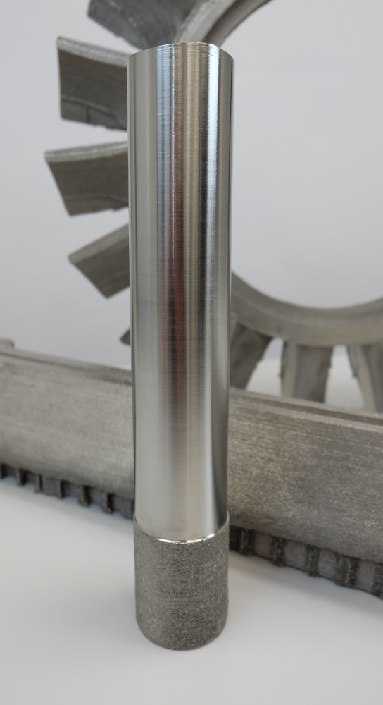
Markus Ramsperger from GE Additive Arcam EBM Center of Excellence, Sweden, reported on PBF-EB of the non-weldable nickel-based superalloy Alloy 247 for high-temperature applications, such as turbine blades in aero-engines [23], Fig. 14 (left). In addition to building defect- and crack-free material, the goal of the study was to tailor the microstructure depending on application requirements, which is a unique capability of the PBF-EB process, Ramsperger said, and echoing the sentiment of Karimi from the University of Waterloo in Canada.
The complex crack formation in this alloy in Additive Manufacturing, which was originally designed for casting, is based on different effects. Among them are rapid solidification, which results in high residual stresses, superimposing with partly remelted microstructure, plus segregation effects and the issue that in-situ heat treatment further develops the microstructure in case of carbides and gamma prime phases. Ramsperger mentioned the use of PBF-EB and advanced scanning strategies to influence the shape of the melt pool and thus the solidification, on the one hand, and thermal balance during processing, on the other hand. In this way, the temperature gradient can be influenced, he explained.
Final experiments were done on an ArcamEBM SpectraH machine from GE Additive, with its improved electron beam unit, software and temperature monitoring. The resulting microstructures ranged from equiaxed to columnar grains, as shown in Fig. 14 (right). While deep and sharp melt pools supported polycrystalline (PX) microstructures based on equiaxed and elongated grains, broad and flat melt pools rather led to directionally solidified, highly anisotropic, columnar grained microstructures (DS).
Furthermore, Ramsperger showed the feasibility of using the PBF-EB process to produce single crystalline microstructures (SX) from Alloy 247 on test structures. Subsequent Hot Isostatic Pressing, followed by a solution heat treatment at temperatures up to 1,295°C and a two-step ageing, should further improve the mechanical properties. The resulting material generally yielded superior high-temperature properties, especially for fracture elongation above 500°C, in comparison to other Additive Manufacturing technologies.
For the polycrystalline microstructure, tensile strength was additionally measured and this exceeded those of the conventionally cast alloy, Ramsperger said. Finally, and most importantly for this material, the creep properties of the Additively Manufactured DS microstructure were comparable to those of cast directionally solidified material, which is still the benchmark.
Conclusion
In conclusion, the EBAM2023 conference highlighted the rising interest in electron beam-based Additive Manufacturing, due to the emerging innovations in machine technology and process observation as well as capabilities in alloy design through machine software, process strategies and computer-aided developments. These topics were combined with other focus discussions such as powder or materials qualification.
This gives rise to many questions. How can we further improve process observation technologies and the interpretation of the measured data? When and how can developments on process monitoring actively feedback into the process to enable process control?
How can promising approaches, such as locally adapted grain morphologies, graded structures or multi-materials, gain acceptance in the industrial landscape? How will existing standards and specifications be addressed, in that case, and how are such components to be tested? How do machine suppliers position themselves to make the transfer of materials among one another as simple as possible and, thus, accelerate the industrial establishment of the process?
Will the new freedom in process control promote alloy development towards EBAM-only materials? Is virtual material alloy-design increasingly going to replace experimental validation?
It remains exciting to see how these and numerous other open issues will progress. What is certain is that they will be discussed at the next EBAM2025.
Authors
Marie Franke-Jurisch
Fraunhofer Institute for Manufacturing Technology and Advanced Materials IFAM, Department Additive Manufacturing, Dresden
Germany
[email protected]
www.ifam-dd.fraunhofer.de
Dr Matthias Markl
Friedrich-Alexander-Universität Erlangen-Nürnberg FAU
Department of Materials Science and Engineering for Metals, Erlangen
Germany
[email protected]
www.wtm.tf.fau.de
www.ebam.fau.de
References
[1] Andrey V. Koptyug, Are we already utilizing everything electron beam melting can deliver?
[2] Dmitriy Khrapov, Aleksandra Paveleva, Maria Kozadayeva, et al., Materials Science and Engineering: A 862, 2023, 144479, https://doi.org/10.1016/j.msea.2022.144479
[3] William Sjöström, Andrey Koptyug, Lars-Erik Rännar, and Carlos Botero, Materials and Manufacturing Processes, 2023, Near-infrared radiation: A promising heating method for powder bed fusion, https://doi.org/10.1080/10426914.2023.2195910, licensed under CC BY 4.0 (http://creativecommons.org/licenses/by/4.0)
[4] Ulf Ackelid, Pixelmelt® software for generating innovative beam scanning patterns in E-PBF
[5] Christoph Breuning, Jonas Böhm, Matthias Markl, Carolin Körner, PBF-EB process strategies on freely programmable machines
[6] Paria Karimi, Esmaeil Sadeghi, Yasmine Hemmati, Shahriar Imani, Katayoon Taherkhani, Ehsan Toyserkani, Towards microstructure engineering via electron beam powder bed fusion
[7] Martyn Hussey, Ian Laidler, Matthew Harvey, Jaap van den Berg, Andrew Rossall, S. Wilson, Active charge neutralisation in ‘NeuBeam’ electron beam PBF
[8] Camilo Medina Viramontes, Ulric Ljungblad, Ulf Ackelid, ProHeat® – a new heating method for electron beam powder bed fusion, opening a wider range of processable feedstocks
[9] Ralf Edinger, Will Sparling, Chad W. Sinclair, Powder properties in EBAM: processing impacts and opportunities
[10] Dongfang Wang, Dechen Zhao, Xiaoyu Liang, Xiang Li, Feng Lin, The investigation on the evolution of smoking phenomenon in electron beam powder bed fusion process
[11] Sebastian Pohl, Alexander Klassen, Leonardo Sansonetti, EBM machine concept for industrial serial production
[12] Fuad Osmanlic, Michael Kordik, Robert Hönig, Klaus Löser, EBuild® 850: industrial scale electron beam powder bed fusion
[13] Feng Lin, Wenbin Kan, J. Wang, D. Zhao, L. Liu, The efforts on new machine development to promote the size and efficiency of electron beam powder bed fusion process
[14] Christian Haase, Design of alloys for additive manufacturing by efficient combination of experiments, simulation and machine learning
[15] Patrick Köhnen, Simon Ewald, Johannes Henrich Schleifenbaum, Andrey Belyakov, Christian Haase, Controlling microstructure and mechanical properties of additively manufactured high-strength steels by tailored solidification, Additive Manufacturing 35, 2020, 101389, https://doi.org/10.1016/j.addma.2020.101389
[16] Marc Ackermann, Christian Haase, Machine learning-based identification of interpretable process-structure linkages in metal additive manufacturing, Additive Manufacturing 71, 2023, 103585, https://doi.org/10.1016/j.addma.2023.103585
[17] Christopher Arnold, Christoph Breuning, Carolin Körner, Process Monitoring by Evaluation of Backscattered Electrons during Electron Beam Melting, EBAM 2020 Conference, 2020
[18] Christopher Arnold, Fundamental Investigation of Electron-Optical Process Monitoring in Electron Beam Powder Bed Fusion, Dissertation, 2023, https://nbn-resolving.org/urn:nbn:de:bvb:29-opus4-216113
[19] Jakob Renner, Matthias Markl, Carolin Körner, Electron optical imaging with multi-detector systems for process monitoring and control applications
[20] Jakob Renner, Christoph Breuning, Matthias Markl, Carolin Körner, Surface topographies from electron optical images in electron beam powder bed fusion for process monitoring and control, Additive Manufacturing 60, Part A, 2022, 103172, https://doi.org/10.1016/j.addma.2022.103172, licensed under CC BY 4.0 (http://creativecommons.org/licenses/by/4.0)
[21] Frauke Hinrichs, Daniel Schliephake, Sascha Seils, Susanne Obert, Alexander Kauffmann, Karin Ratschbacher et al., Flexible powder production for additive manufacturing of refractory metal alloys
[22] Frauke Hinrichs, Alexander Kauffmann, Daniel Schliephake, Sascha Seils, Susanne Obert, Karin Ratschbacher et al., Flexible powder production for additive manufacturing of refractory metal alloys, Metals 11, 2021, 1723, https://doi.org/10.3390/met11111723, licensed under CC BY 4.0 (http://creativecommons.org/licenses/by/4.0)
[23] Markus Ramsperger, Electron beam melting as an enabler for difficult to process materials
[24] Markus Ramsperger, Simon Eichler, Electron Beam Based Additive Manufacturing of Alloy 247 for Turbine Engine Application: From Research towards Industrialization, Metallurgical and Materials Transactions A 54, 2023, 1730–1743, https://doi.org/10.1007/s11661-022-06955-0, licensed under CC BY 4.0 (http://creativecommons.org/licenses/by/4.0)
LAST MONTH’S MOST-READ ARTICLES