

Enabling the fusion energy revolution: Mastering tungsten with PBF-EB Additive Manufacturing
There is a growing interest in additively manufactured pure tungsten, primarily propelled by the expected demand for tungsten components in future fusion power plants. Here, Additive Manufacturing veterans and PBF-EB enthusiasts, Ulf Ackelid and Ulric Ljungblad – both of Sweden’s Freemelt AB – provide insights into the AM of tungsten and the benefits of using an electron beam as the energy source. This article is a standalone continuation of previous PBF-EB articles in Metal AM, published in the Summer 2020, Autumn 2022, and Summer 2023 issues. [First published in Metal AM Vol. 10 No. 3, Autumn 2024 | 20 minute read | View on Issuu | Download PDF]

Tungsten is an element with Swedish and Spanish heritage. The famous Swedish chemist, Carl Wilhelm Scheele, identified tungsten (the name is a portmanteau of the Swedish words for heavy stone, ‘tung’ and ‘sten’) in 1781 as the major constituent of the ore scheelite, later identified as calcium tungstate (CaWO4). Two years later, the Spanish chemist brothers, José and Fausto de Elhuyar, found a reduction process that isolated pure tungsten metal from its wolframite ore. To this day, tungsten maintains its original Swedish name in major languages such as Spanish, English, and French, whereas the Swedes have adopted the German word ‘wolfram.’ The name wolfram is the origin of tungsten’s chemical symbol W.
Tungsten has several outstanding material properties that make it industrially useful. It is classified as a refractory metal and has the highest melting point of all elements, 3,422°C, making it extremely heat resistant. It also has the lowest thermal expansion of all elements. Its density is as high as gold and seven times higher than aluminium. The X-ray shielding properties of tungsten are excellent, better than lead and without the environmental concerns and toxicity. Tungsten is also a good conductor of heat and electricity, is non-magnetic and has high hardness, and excels in wear resistance as well as corrosion resistance. All in all, tungsten is a unique metal.
Tungsten and tungsten alloys are used in a multitude of applications, such as heat resistant metal components, medical X-ray shielding equipment, X-ray sources, rocket engine parts, heating elements in furnaces, ammunition and armour-piercing projectiles, counterweights/ballasts for vehicles and aircraft, jewellery and welding electrodes. Tungsten is also important industrially as a constituent in tungsten carbide tools and other applications for metalworking, but that is beyond our present scope.
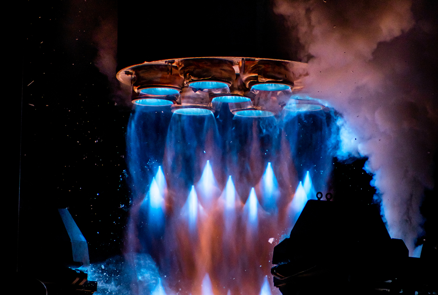
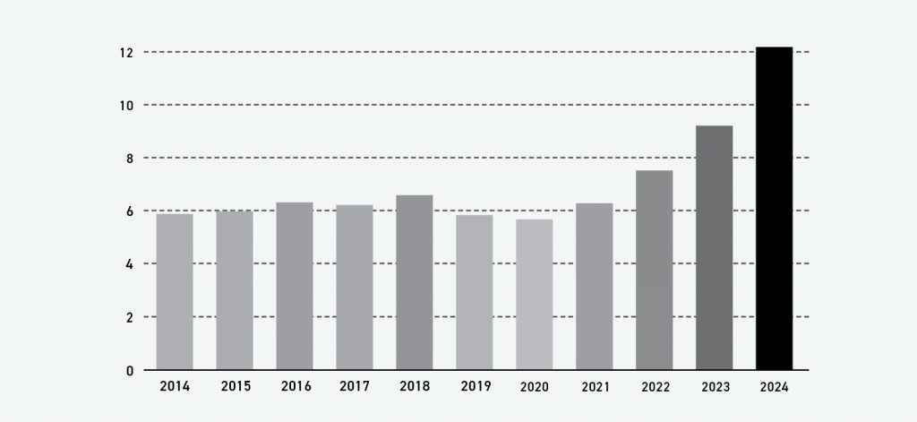
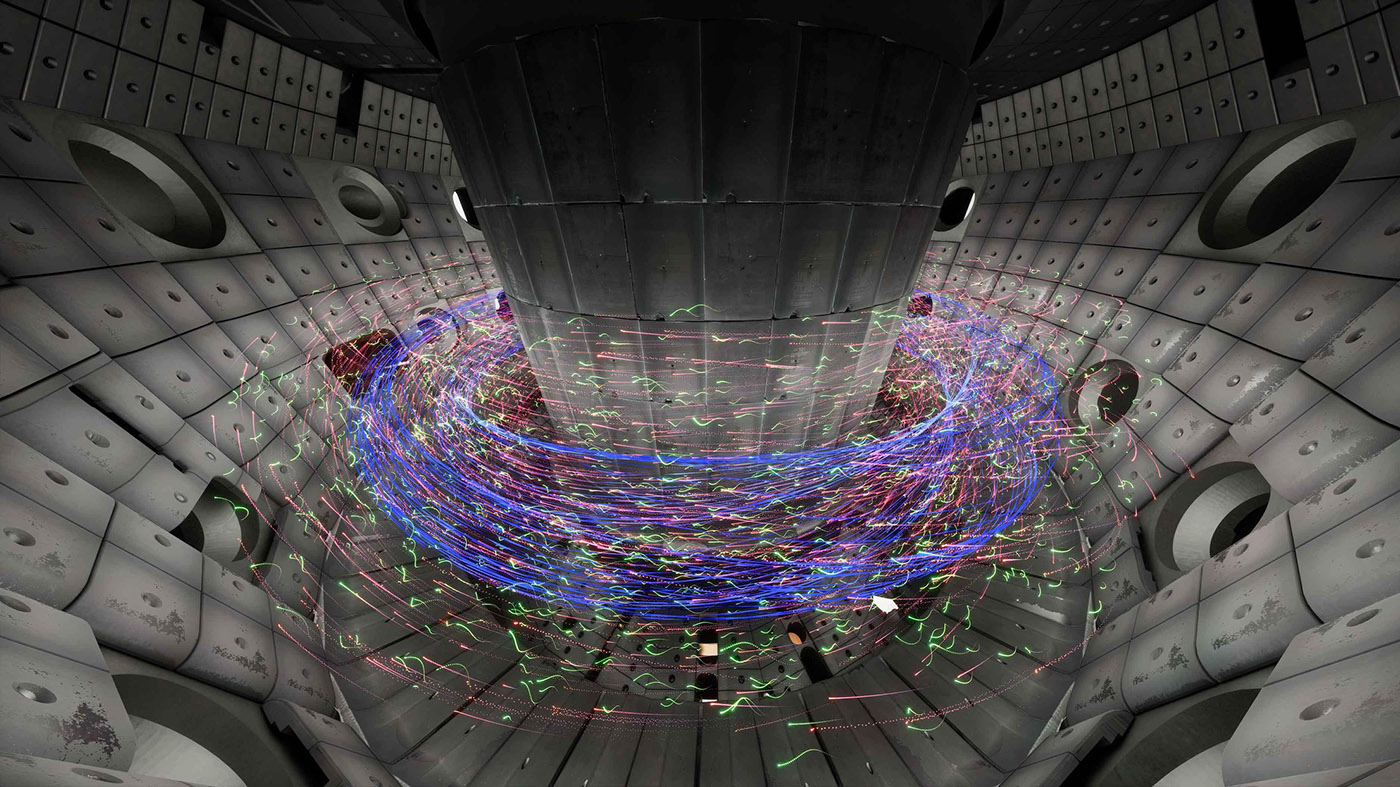
More relevant to our current audience is the fact that fusion energy is gaining increasing interest, and tungsten has crystallised into the prime candidate for plasma-facing components of fusion reactors (Fig. 1). This might be a reason tungsten has doubled in popularity in academic AM publications in the past three years, as indicated by Google Scholar data (Fig. 2).
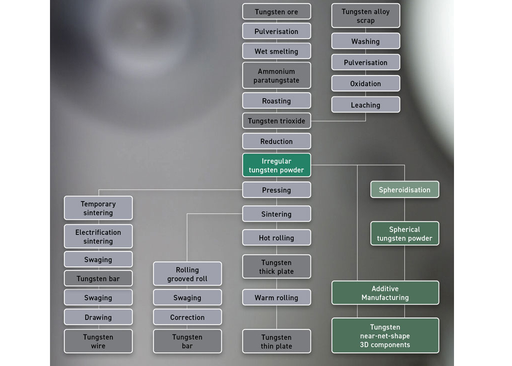
Bulk tungsten metal is virtually impossible to produce via conventional hot melting technology such as casting, simply because there are no solid materials heat resistant enough to enclose molten tungsten safely and inertly. Tungsten is, therefore, consolidated via Powder Metallurgy (PM) methods and non-melt processing such as rolling or swaging. Fig. 3 summarises the conventional routes for wire, bar, and plate production, using either tungsten ore or tungsten metal scrap as the raw material (it should be noted, however, that it is difficult to machine complex shapes from tungsten barstock). The figure also shows the more recent AM route where tungsten powder can be used either in its chemically extracted form or after plasma spheroidisation. Spherical powder shape is preferred in most AM technologies due to its spreadability and packing density, but on the other hand, the spheroidisation of tungsten powder adds substantial cost.
Conventionally made PM tungsten is not all milk and honey, however; some drawbacks have hampered widespread industrial use. PM tungsten often has substantial residual porosity and the material is brittle and notoriously difficult to machine at room temperature. The brittleness is partly inherent in the slip-resistant body-centred cubic crystal structure of tungsten, but is also due to the fact that non-melt PM fabrication always leaves some impurities such as oxygen and carbon. Impurities tend to segregate to grain boundaries and further contribute to brittleness. It should be noted, however, that tungsten becomes ductile at elevated temperatures. The ductile-to-brittle transition temperature (DBTT) has been reported in the interval 200-800°C, depending on microstructure, texture, and impurity level.
Pure tungsten processed by Laser Powder Bed Fusion (PBF-LB)
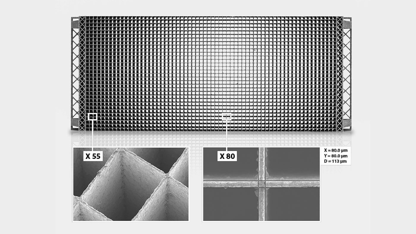
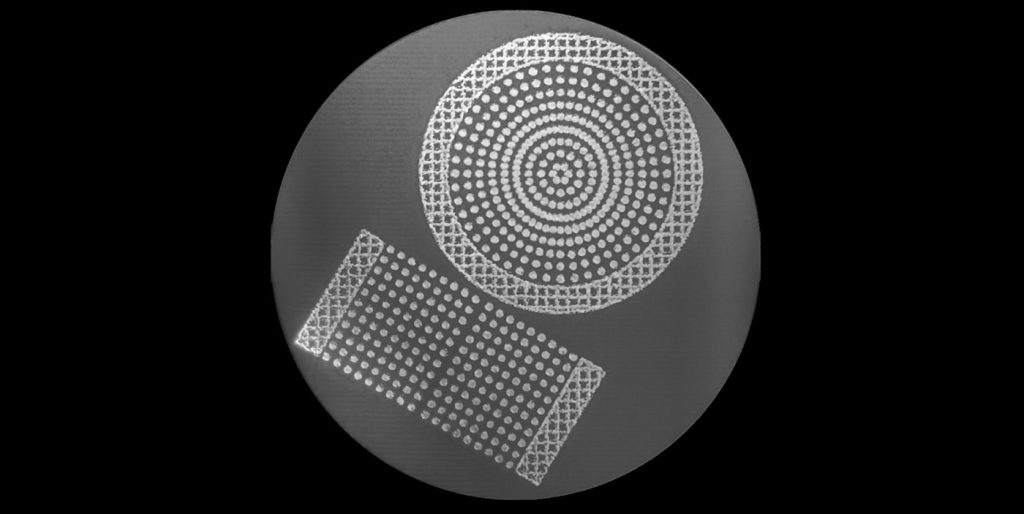
Industrial tungsten manufacturing by PBF-LB has been around for more than a decade. A well-known PBF-LB tungsten manufacturing facility is that of Dunlee in the Netherlands. Dunlee started providing its tungsten Additive Manufacturing services to the market in 2012 and successfully secured a major customer for serial production in 2014. Since then, Dunlee’s business has grown with several successful tungsten applications being added to their portfolio. Their most well-known product is antiscatter grids for X-ray CT systems used in medical imaging, as shown in Fig 4. These grids are designed to absorb the X-ray scatter before reaching the detector, ensuring enhanced image quality, and they contain walls in pure tungsten as thin as 70 µm. It is obvious that such detailed geometries could not be produced by conventional PM routes. Without knowing their exact number of PBF-LB machines, it is believed that Dunlee operates the largest fleet of AM equipment dedicated to tungsten in Europe, and possibly in the world.
On the PBF-LB research side, there have been numerous studies exploring tungsten manufacturability [1-6]. There is a clear consensus that, while PBF-LB can make sub-millimetre thin-wall tungsten structures such as shown in Fig. 4, it struggles with dense material in thicker and bulkier shapes. As PBF-LB parameters are optimised for low bulk porosity, microcracks appear in PBF-LB tungsten, and the main reason is accumulated stress as the melt pool cools down to the brittle temperature regime of tungsten, far below the DBTT. Fig. 5 shows an example of such cracks. A few attempts have been described where the PBF-LB build platforms were heated up to 1,000°C [7], but some cracks persisted even at such high build temperatures. A hot build platform introduces another problem: the high propensity of hot tungsten to pick up impurities from the shielding gas in the PBF-LB machine. As already mentioned, impurities in tungsten will further increase its brittleness.
![Fig. 5 Microstructure cross-section of a 5 mm thick tungsten specimen fabricated with PBF-LB, illustrating the characteristic network of intergranular cracks commonly described in the literature (from [4], with permission)](http://www.metal-am.com/wp-content/uploads/sites/4/2024/12/fig-05-1024x652.jpg)
In conclusion, the authors are unaware of any established solution for manufacturing dense and crack-free parts of arbitrary bulky shape in pure tungsten using PBF-LB.
Pure tungsten processed by Electron Beam Powder Bed Fusion (PBF-EB)
PBF-EB distinguishes itself from PBF-LB by some features that could be beneficial for tungsten. Thanks to the heat insulation of the vacuum used inside PBF-EB machines, the powder bed can easily be kept at glowing hot temperatures to relieve stress and reduce the risk of cracking, and the vacuum is also a very clean environment helping to keep the tungsten free of impurities.
There are some good review papers covering PBF-EB tungsten studies [2, 3, 6]. The pioneer was Jonathan Wright at the University of Sheffield in the UK, who processed pure tungsten in 2015 as the start of his PhD project [4]. His project involved a direct comparison between PBF-EB and PBF-LB using the same plasma-spheroidised powder of typical laser size (25-45 µm). For PBF-EB, high-density and crack-free tungsten was successfully produced with the build platform temperature continuously maintained at ≈1,000°C. For PBF-LB, high density specimens could also be made at the maximum beam power of 400 W, but at the expense of cracks (Fig. 5). Wright’s PhD thesis also provided the first demonstration of more complex PBF-EB geometries, such as the beautiful tungsten lattice toroid in Fig. 6. All Wright’s PBF-EB work was done in an Arcam S12 machine.
![Fig. 6 Early demonstration lattice toroid built with PBF-EB at the University of Sheffield in 2016. The outer diameter is 80 mm (from [4] with permission)](http://www.metal-am.com/wp-content/uploads/sites/4/2024/12/fig-06-web-1024x554.jpg)
Another institution that has contributed significantly to PBF-EB tungsten development is Oak Ridge National Laboratory (ORNL) in Tennessee, USA. ORNL is the largest national laboratory under the US Department of Energy, and one of its focus areas is sustainable energy sources of the future, such as fusion power. ORNL has been continuously active in PBF-EB materials research for 15 years and refractory metals have been the main effort for the past five years.
ORNL has explored powder bed temperatures as high as 1,800°C to find the optimum conditions for tungsten processing. The team has seen that the oxygen content drops as the tungsten powder is fused by the electron beam, and single ppm levels of oxygen have been reported in the built material. This seems very promising to counteract brittleness. The organisation further reports that its dense and crack-free PBF-EB tungsten has good tensile properties at high temperatures, resembling high-quality PM tungsten in its annealed and recrystallised state.
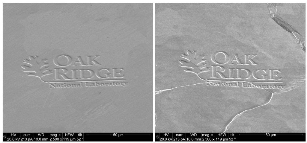
In May 2023, PBF-EB specimens built by ORNL were exposed to combined high heat and particle fluxes in the DIII-D National Fusion Facility in San Diego, to assess their plasma-facing material response in comparison with conventionally made recrystallised tungsten of high purity [9]. Fig. 7 shows scanning electron micrographs before and after the exposure. PBF-EB tungsten exhibited some surface roughening, grain growth and crack initiation, but less severe than the reference specimen. The PBF-EB specimens did not exhibit unique failure modes such as flaking or material ejection. In conclusion, PBF-EB tungsten demonstrated comparable or better results in terms of thermo-mechanical response and surface damage.
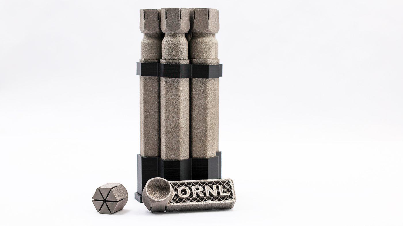
ORNL has also demonstrated its tungsten processing capability in test geometries relevant to fusion energy. Fig. 8 shows hexagonal tile geometry, which represents a tile for potential use in the diverter or inner wall of a Tokamak fusion reactor. The tiles are mounted on additively manufactured rods with internal passages for flowing cooling gases to the tiles.
![Fig. 9 PBF-EB tungsten samples built in the EUROfusion study (top photo). Mock-up for high-heat-flux testing, made by PBF-EB tungsten and copper infiltration (above photo) (Copyright © 2024 Karlsruhe Institute of Technology, CC-BY-4.0 [10])](http://www.metal-am.com/wp-content/uploads/sites/4/2024/12/fig.9-updated-for-web-1024x308.jpg)
The plasma-facing properties of PBF-EB tungsten have also been investigated recently in Europe, within the framework of the EUROfusion Consortium [10]. A team led by Karlsruhe Institute of Technology in Germany fabricated tungsten specimens via PBF-EB and combined them with novel copper cooling structures (Fig. 9). The tungsten specimens were exposed to various tests simulating fusion reactor conditions. They survived thermal shock testing in the JUDITH facility in Jülich without macroscopic failure. They also withstood the exposure to high heat fluxes at the GLADIS facility in Garching, with some near-surface grain growth as the only concern. A new test campaign with optimised geometries and improved cooling structures is in the pipeline.
Note that [10] also contains a general material characterisation of PBF-EB tungsten compared with reference material in rolled PM tungsten. The density was 99.8% and the microstructure was columnar and crack-free. Thermal conductivity and thermal diffusivity were similar to the reference material. Hot tensile testing at 600-1,000°C showed ductile behaviour with extraordinary elongation up to 80%.
Freemelt’s approach to tungsten AM using PBF-EB
Freemelt AB is an AM technology supplier founded in 2017 in Mölndal, Sweden. The founding team had profound experience of PBF-EB from previous employment at Arcam AB (later GE Additive, now Colibrium Additive). Freemelt’s initial business idea was to develop a small and powder-lean PBF-EB machine with open-source software, targeting universities and research institutes. This machine – the Freemelt® ONE – was launched in 2019 and has since been sold to several R&D users in Europe, North America and Asia. Freemelt ONE has many tailored features for advanced AM research, such as freely programmable beam scanning and multiple ports for user-defined process monitoring, and it can be operated with powder quantities as small as two kilograms.
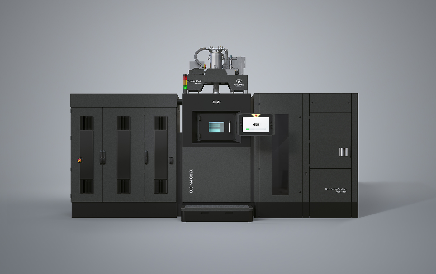
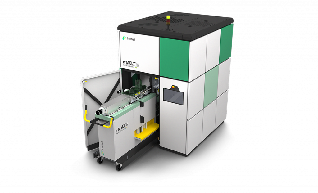
Freemelt tried tungsten powder in Freemelt ONE for the first time in 2021 and quickly got promising results. At the same time, development commenced on a new PBF-EB machine series, e-MELT®, based on the same core technology and open-source platform as Freemelt ONE. eMELT is targeting serial production and is based on progress with tungsten processing and, based on an increasing number of enquiries for the material, tungsten was selected as a priority material for this machine. The eMELT-iD, shown in Fig. 10, the first machine in the eMELT series, has recently been delivered to Italy and a second order has been received from the US. eMELT-iD is intended for application development and initial production and will be followed by an even more productive machine.
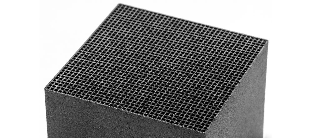
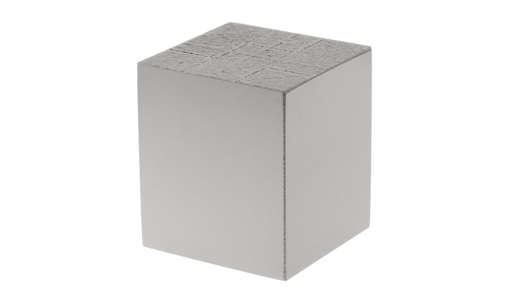
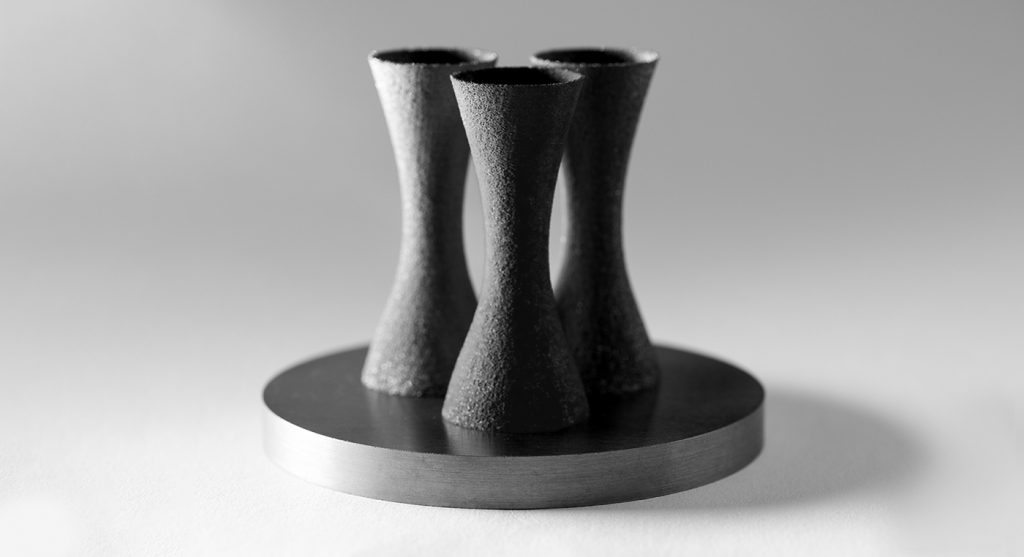
Freemelt machines are capable of manufacturing high-density, crack-free tungsten parts with thick and thin cross sections. Fig. 11 shows a tungsten cube that has been post-polished to mirror finish on the side surfaces. Despite its basic geometry, this cube attracted a lot of attention in the Freemelt booth at Formnext 2023, simply because nobody had seen such a massive piece of AM tungsten before. Further examples of thin-walled tungsten geometries are seen in Fig. 12 and Fig. 13. There are several features in the eMELT machines that make them particularly suited for PBF-EB production of tungsten parts.
A grid-less electron gun based on a ‘diode’ design
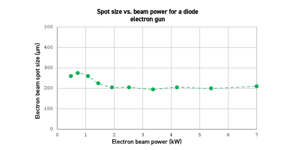
Freemelt has developed its own grid-less electron gun based on a ‘diode’ design which has a stable beam spot size over the full beam power range from 0-6 kW, as shown in Fig. 14. This is in contrast to the common ‘triode’ electron gun used in other PBF-EB machines, which has its sweet spot at low beam power and gradually deteriorating beam quality at higher beam power [11]. The diode electron gun is an advantage for tungsten processing, since the tungsten powder bed temperature is kept above 1,200°C. The diode electron gun can melt the powder layers at higher beam power which also contributes to the heating needed to maintain the powder bed at 1,200°C. Thus, less beam time will be needed for the heating sequence normally used in hot PBF-EB processes. This translates to higher productivity.
Active cooling of the build tank during and after the process
To the authors’ knowledge, the eMELT machines are the first on the market to offer active water cooling of the build tank during and after the process. This contributes to higher productivity for two reasons. By continuous cooling during the process, even higher melt power and higher melt speeds can be used without the risk of overheating the powder bed. After the build is completed, the water cooling drastically reduces the post-cooling time down to room temperature. A common argument against PBF-EB in the past has been that post-cooling requires many hours of unproductive time. With active water cooling, the post-cooling time is reduced to ≈ 30 minutes for a build run at 1,200°C, if desired. This cooling principle is particularly efficient for tungsten, because of tungsten’s very high thermal conductivity. The heat accumulated in the tungsten powder bed is quickly conducted to the water-cooled walls of the build tank.
A modular approach
Unique to eMELT is a dockable build module, as depicted in Fig. 10. The build module is a separable unit containing the build tank as well as the powder feeding system. An eMELT machine can be equipped with double build modules, so that one module can be in use for building tungsten parts while the second module is emptied, reloaded with powder and prepared for the next build in a standalone turnaround station. This docking concept helps to reduce the dead time between builds to a minimum and, of course, it contributes to higher productivity.
The importance of vacuum quality
An advantage when processing tungsten is superior vacuum quality. As previously mentioned, hot tungsten easily picks up oxygen from uncontrolled processing environments, jeopardising the material quality. The eMELT series offers the smallest vacuum chamber volume on the market, equipped with double turbomolecular pumps. This translates to a very short pump downtime and a processing vacuum as low as 10-5 mbar. This is an extremely clean environment, orders of magnitude better than a high-purity inert gas typically used in a PBF-LB machine. It should also be noted Freemelt technology allows tungsten to be processed without the small helium or argon bleed that is commonly used in other PBF-EB solutions. It has been observed that our clean PBF-EB vacuum conditions not only prevent oxygen pickup in tungsten – they actually purify the tungsten from oxygen as the material is fused. Single ppm levels of oxygen have been reached in the final tungsten material, which is remarkable and promising for maximum cracking resistance.

Spot melting technology
An electron beam can be scanned at very high speed (kilometres per second) over a powder bed. This opens up the potential of ‘spot melting’ for tungsten processing. In the past, PBF-LB and PBF-EB have traditionally employed so-called ‘line melting’ or ‘raster melting,’ where the powder layer is melted along adjacent lines using a continuously moving melt pool.
In spot melting, the electron beam melts the powder layer in a discrete fashion, creating sub-millimetre melt pools that solidify individually. The time to create one melt pool is typically in the microsecond to millisecond range, and beam jumping between melt pools is virtually instantaneous. Thus, the electron beam can create thousands of melt pools in one second.
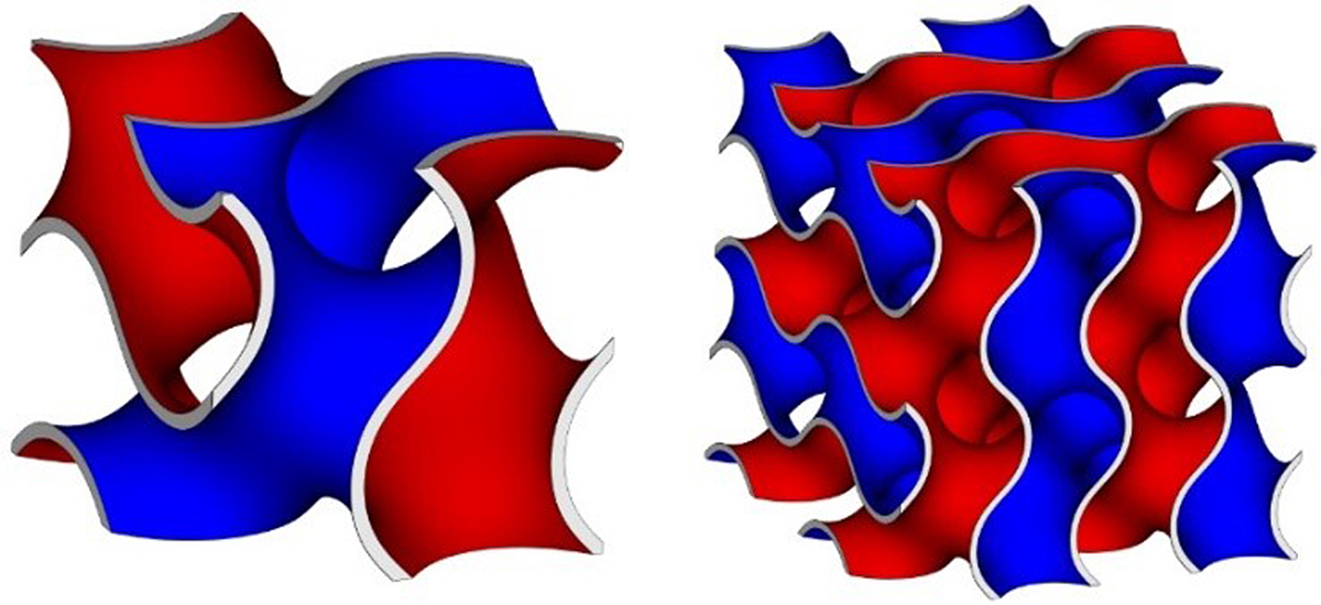
Freemelt has developed a software solution called Pixelmelt® that assists in creating various spot melting algorithms. Figures 15 and 16 show different Pixelmelt patterns used in its tungsten builds. Fig. 15 is an ordered pattern where melt pools were created at constant beam jump distance from each other. Fig. 16 is a seemingly unordered pattern where the melt pools were distributed according to user-defined rules. Spot melting is beneficial for tungsten because it can distribute the heat evenly over the melt area, which reduces the risk of residual stress. Spot melting also eliminates the risk of macroscopic swelling that could appear for conventional line melting at very high beam powers. And, even more exciting, different spot melting algorithms will produce different microstructures in tungsten, opening up the possibility of site-specific microstructure tailoring. Based on all these benefits, it is expected that spot melting will become mainstream in PBF-EB in the near future.
In-situ process monitoring
Freemelt machines are equipped with an electron detector that collects electrons backscattered from the powder bed during processing. The electron signal is converted to an image, according to the same principle as in scanning electron microscopes. Tungsten has a very high electron emission due to its high atomic number (Z=74), and thus tungsten produces excellent electron images with high contrast and good signal-to-noise ratio. An example of an electron image is shown in Fig. 17. Such images stacked on top of each other can produce a 3D image of the whole build, showing internal porosity and other potential problems. This is particularly useful for tungsten which is notoriously difficult to examine ex-situ with non-destructive testing methods such as X-ray computer tomography. Electron imaging is a robust technology that copes well with the demanding conditions in a tungsten PBF-EB machine where heat radiation, metal vapour and X-rays prevail.
A new level of interest in the AM of tungsten
In the past year, Freemelt’s tungsten development has entered a new phase. A number of collaborations have been initiated with institutions and companies to further explore and accelerate PBF-EB tungsten opportunities for fusion energy and other strategic areas. In Europe, projects are running together with the UK Atomic Energy Authority, the Nuclear Advanced Manufacturing Research Centre at the University of Sheffield, Mid-Sweden University, Sandvik and WEAREAM, just to name a few. In North America, Georgia Tech Manufacturing 4.0 Consortium, Texas A&M Engineering Experiment Station and North Carolina State University are collaborators, together with several undisclosed private initiatives. It is uplifting and encouraging to see such a wide interest in additively manufactured tungsten, and new results from Freemelt partners are expected to be published in the near future.
Summary and outlook
Tungsten has a rich history, unique material properties and a multitude of potential uses. Tungsten applications related to sustainable energy production and defence are attracting particular interest these days, for obvious reasons, but tungsten is unfortunately a difficult material in terms of conventional fabrication and machining. With this background, it is not surprising that tungsten is on the rise within the worldwide AM community. Additive Manufacturing opens up new possibilities of manufacturing complex 3D parts in tungsten. There is also a great potential to improve chemical purity and the density, and eliminate the defects seen in tungsten made by conventional Powder Metallurgy.
In this article, ongoing efforts to develop PBF-LB and PBF-EB technology for pure, unalloyed tungsten have been described. Arguments in favour of PBF-EB have been made, particularly for thicker tungsten parts where PBF-LB has struggled with microcracking, porosity and low productivity. Plasma-facing tiles for fusion reactors are a great example where PBF-EB tungsten could excel in the future. That said, PBF-LB may still be a good choice for tungsten applications requiring thin walls, fine details and the highest resolution, particularly if volumetric build rate is not an issue.
Yes, one could argue that we are biased since we are working for a PBF-EB technology supplier, but we are also keen scientists closely following the AM progress at R&D institutions around the world. We do believe that Additive Manufacturing will revolutionise tungsten manufacturing, and we see that the present knowledge favours PBF-EB. Only time will tell where we are going.
References
[1] B. Liu et al., A review on manufacturing pure refractory metals by selective laser melting, https://doi.org/10.1007/s11665-024-09693-z
[2] A. Talignani et al., A review on additive manufacturing of refractory tungsten and tungsten alloys, https://doi.org/10.1016/j.addma.2022.103009
[3] M. Zarinejad et al., Advancements and perspectives in additive manufacturing of tungsten alloys and composites: challenges and solutions, https://doi.org/10.3390/cryst14070665
[4] J. Wright, Additive manufacturing of tungsten via selective laser melting and electron beam melting, PhD thesis, University of Sheffield, https://etheses.whiterose.ac.uk/26247
[5] M.S. Seyam et al., Laser powder bed fusion of unalloyed tungsten: A review of process, structure, and properties relationships, https://doi.org/10.3390/met12020274
[6] P. Morcos et al., Review: additive manufacturing of pure tungsten and tungsten-based alloys, https://doi.org/10.1007/s10853-022-07183-y
[7] A. v. Müller et al., Additive manufacturing of pure tungsten by means of selective laser beam melting with substrate preheating temperatures up to 1000°C, https://doi.org/10.1016/j.nme.2019.02.034
[8] L. Howard et al., Progress and Challenges of Additive Manufacturing of Tungsten and Alloys as Plasma-Facing Materials, https://doi.org/10.3390/ma17092104
[9] J. Coburn et al., High Heat Flux Exposures of Recrystallized and Additively Manufactured Tungsten Samples on DIII-D, https://meetings.aps.org/Meeting/DPP23/Session/TO08.9
[10] S. Antusch et al., Additive manufacturing of novel complex tungsten components via electron beam melting: Basic properties and evaluation of the high heat flux behavior, https://doi.org/10.1016/j.nme.2024.101683
[11] M. Reith et al., Impact of the Power-Dependent Beam Diameter during Electron Beam Additive Manufacturing: A Case Study with γ-TiAl, https://doi.org/10.3390/app122111300
Authors
Ulf Ackelid, Ph.D., Principal Scientist, and Ulric Ljungblad, Chief Innovation Officer
Freemelt AB
Bergfotsgatan 5A
SE 431 37 Mölndal
Sweden
[email protected]
www.freemelt.com
LAST MONTH’S MOST-READ ARTICLES