

AMPM2016: New material developments in metal Additive Manufacturing technology
In the second of our reports from the Metal Powder Industries Federation’s Additive Manufacturing with Powder Metallurgy (AMPM) conference, Dr David Whittaker reports on three presentations that highlighted developments in the processing of novel AM materials. These include tungsten for nuclear fusion applications and copper alloys for applications which require high electrical conductivity. [First published in Metal AM Vol. 2 No. 3, Autumn 2016 | 20 minute read | View on Issuu | Download PDF]
![Fig. 1 Nuclear fusion is a promising option for generating large amounts of low carbon energy [1]](http://www.metal-am.com/wp-content/uploads/sites/4/2016/09/01-2-1024x714.jpg)
Additive Manufacturing of tungsten
Extending the reach of metal Additive Manufacturing into new material types was the focus of a number of contributions to the AMPM2016 programme. A presentation from Jonathan Wright (University of Sheffield, UK), co-authored by Iain Todd (also University of Sheffield), focused on the Additive Manufacturing of tungsten, with particular reference to components for nuclear fusion reactors.
Nuclear fusion mimics the process of energy generation in the sun and involves the collision of nuclei of the isotopes of hydrogen (deuterium and tritium), causing them to fuse together to form helium nuclei and release energy in the form of neutrons. There is significant interest in the potential development of nuclear fusion because, unlike nuclear fission, the process generates no long-lived radioactive waste.
The temperatures involved in nuclear fusion are very high (100 million °C). The most promising means of achieving these conditions is ‘magnetic confinement’ of the hot gas, as a plasma, in a ring-shaped magnetic chamber known as a tokamak (Fig. 1). A tokamak, developed at the Joint European Torus (JET) at Culham, UK, has produced 16 megawatts of fusion power and proved its technical feasibility using deuterium and tritium. The challenge now is to prove that fusion can work on a power plant scale. International fusion research is following a roadmap to achieve power generation within 30 years. The next stage in this programme is ITER (the International Tokamak Experimental Reactor), a multinational project at Cadarache in the south of France. ITER will be a 500 megawatt tokamak, equivalent to a small power plant.

Tungsten has emerged as one of the prime candidate materials for the plasma facing components in a tokamak in the next generation fusion plant (ITER), because of its high level of melting point (3683°C), thermal conductivity (174 W/mK) and thermal diffusivity (6.9 x 10⁻⁵). However, because of its high hardness (900 Hv), tungsten is problematic to machine and, therefore, net- and near-net -shape manufacturing technologies are of significant interest. In this context, therefore, Additive Manufacturing is of potential interest and the reported study related to the assessment of the viability of the Additive Manufacturing technologies, Selective Laser Melting (SLM) and Electron Beam Melting (EBM), in this context.
![Fig. 2 The divertor is used to remove waste products and extract heat via active cooling [1]](http://www.metal-am.com/wp-content/uploads/sites/4/2016/09/02-2-822x1024.jpg)
The target application was referred to as a divertor, a component used to remove waste products from the system and extract heat via active cooling (Fig. 2). The SLM study used a Renishaw SLM 125 machine, operating with a pulsed 200 W laser and an argon atmosphere. A full factorial design of experiment study was carried out, with the variables being layer thickness, beam speed and hatch spacing. The results were presented in the form of contour plots of % porosity versus layer thickness and exposure time (Fig. 3). The conclusions drawn were that 95% density was achievable, but that this was limited by layer thickness and power density. The results suggested that, to reduce porosity, higher energy density is needed via either thinner layers or higher beam power. This part of the presentation led to the conclusion that, for SLM, further process optimisation was required.
![Fig. 3 Contour map of achievable porosity level versus layer thickness and exposure time [1]](http://www.metal-am.com/wp-content/uploads/sites/4/2016/09/03-1-1024x681.jpg)
EBM was studied using the ARCAM Electron Beam Melting process, which involves pre-heating the build plate and powder bed (to 1000°C) and operation in vacuum. Fig. 4 shows a schematic of the process. The advantage of EBM over SLM is that much higher beam power is available (3000 W cf. 200 W). The disadvantage is that the standard ARCAM machine has a large build tank and, therefore, a large powder volume is required.
![Fig. 4 Schematic of the EBM process [1]](http://www.metal-am.com/wp-content/uploads/sites/4/2016/09/04-1-1024x745.jpg)
The first stage of this work was the development of the process to operate with a small build tank (Fig. 5). Initially, the small build tank was evaluated with Ti-6Al-4V powder. The issues identified were heat loss, leading to the creation of smoke or hard sintering, and, as the time for the beam to cover the plate is faster, again smoke generation is a problem. The developed solutions were to maintain the energy density and beam return time in preheating and to introduce additional heating steps during the melt stage to counteract heat loss without raising the maximum layer temperature.
![Fig. 5 Small build tank for EBM [1]](http://www.metal-am.com/wp-content/uploads/sites/4/2016/09/05-1-1024x675.jpg)
Following this optimisation work, the EBM of tungsten was studied, with a build temperature of around 1000°C, a manual preheat, a hatch melt sequence and a build layout with wafer supports. It was found that, with EBM, a density of 99.9% was achievable. It was concluded that EBM could provide a method for simplifying the manufacture of complex geometries in tungsten for the fusion environment. Further work would involve mechanical and thermal testing of built material and the production of test components.
Metallographic characterisation of copper alloys fabricated via SLM
A presentation from Jack Edgerton (Loewy Institute, Lehigh University, USA) reported on the metallographic characterisation of copper alloys fabricated by Selective Laser Melting. The principal author of the reported study was Anthony Ventura (a PhD student in the Loewy Institute) and the study arose from a collaboration involving other colleagues at the Institute and Greg Pawlikowski and Martin Bayes of TE Connectivity, USA.
The project was motivated by the fact that there are limited existing alloy systems in AM technologies to address applications which require high electrical conductivity. The objectives were to understand the role of alloying element segregation in resulting SLM microstructures and to determine the effect of post-fabrication heat treatment on mechanical properties for a copper alloy. The approach chosen was to optimise the density of the as-printed component by varying the process parameters and to characterise the as-built microstructure and properties and the effect of post-processing heat treatments on the microstructure and mechanical properties to determine and understand a window of attainable properties. The post-processing heat treatments applied were:
- A “standard” anneal at 600 °C for 1 hour (Argon atmosphere)
- A high temperature anneal at 900 °C for 1 hour (Argon atmosphere)
The material used was an air atomised Cu-4.3%Sn alloy powder. This material was defined as being similar to a C-510 bronze, but without a phosphorus addition. AM samples were built at TE Connectivity, using an EOS M280 200W DMLS machine.
![Table 1 As-printed and heat treated mechanical properties and conductivities for Cu-4.3%Sn alloy [2]](http://www.metal-am.com/wp-content/uploads/sites/4/2016/09/t01-1024x396.jpg)
The achievable mechanical properties and conductivity in the as-printed and heat-treated conditions are shown in Table 1. In terms of conductivity, the %IACS is based on the resistivity of commercially pure annealed Cu. The measured properties were within the range of currently used conductive alloys. It was concluded that successful and repeatable production of Cu-4.3Sn components via SLM, with reasonable conductivity and a moderate range of mechanical properties, has been demonstrated.
![Fig. 6 Base microstructural characterisation [2]](http://www.metal-am.com/wp-content/uploads/sites/4/2016/09/06-2-1024x393.jpg)
Base microstructural characterisation showed that, in the as-printed condition, grains appear to grow epitaxially from previously un-melted layers (Fig. 6). The IPF results (Fig. 7) showed that annealing at 600 °C had no effect on grain morphology, whereas there was a significant change on annealing at 900 °C. Assessment of dislocation densities in the three conditions tended to mirror the same observations.
![Fig. 7 Grain morphologies with IPF mapping [2]](http://www.metal-am.com/wp-content/uploads/sites/4/2016/09/07-1-1024x421.jpg)
Annular bright field STEM showed oxide particles to be present in the as-printed condition and the authors believed that these particles arise from oxidation on the surface of the source powder. The oxide particles appear to be similar for the as-printed and the 600 °C annealed conditions, but their size had grown after the 900 °C anneal. It was felt that these particles may be acting as grain boundary pinners. TEM analysis across weld lines in the as-built condition showed a change in the cellular sub-structure (Fig. 8). STEM and corresponding EDS mapping of the cellular substructure showed tin segregation remaining after solidification.
![Fig. 8 TEM analysis of a weld line in an as-built sample [2]](http://www.metal-am.com/wp-content/uploads/sites/4/2016/09/08-1-928x1024.jpg)
Significant influences of the thickness of printed samples (Fig. 9) and of various surface finishing treatments (Fig. 10) on as-printed mechanical properties were observed. The as printed surface texture was irregular and showed the presence of a porosity band. The grit blasted sample showed an improved surface finish, some cracking at the surface and a possible beneficial compressive stress at the surface. Hand grinding gave the best surface quality, with a very even finish and no cracking. Electropolishing created greater irregularity than in the as printed condition with a visible porosity band. While ASTM recommended specifications had been used in electropolishing, it was considered that some further process parameter optimisation might be possible. However, this was not within the scope of this project.
![Fig. 9 Effect of as-built sample thickness on the stress-strain properties of SLM Cu4.3Sn [2]](http://www.metal-am.com/wp-content/uploads/sites/4/2016/09/09-1-1024x604.jpg)
![Fig. 10 Effect of surface finish on the stress-strain properties of SLM Cu4.3Sn [2]](http://www.metal-am.com/wp-content/uploads/sites/4/2016/09/10-1024x518.jpg)
Selective laser melting of nickel-base superalloys for turbocharger applications
![Fig. 11 IN713C SLM turbine wheel (Image from ref. 3 and courtesy of Cummins Turbo Technologies) [3]](http://www.metal-am.com/wp-content/uploads/sites/4/2016/09/11-1020x1024.jpg)
Finally, the selective laser melting of nickel-base superalloys for turbocharger applications was the subject of a presentation, made by Charlotte Boig (University of Sheffield, UK) and co-authored by Iain Todd (also University of Sheffield), Michael Burkinshaw (Cummins Turbo Technologies, UK) and Andrew London and Michael Moody (University of Oxford, UK). The aim of the reported study was to define the required process and compositional control for the robust manufacture of defect-free IN713C SLM turbine wheel components (Fig. 11).
![Fig. 12 Defects in SLM IN713C [3]](http://www.metal-am.com/wp-content/uploads/sites/4/2016/09/12-1024x374.jpg)
The identified problem was that SLM is prone to introducing certain defects and the target component is fatigue life limited and therefore very sensitive to the presence of defects. The types of defects that could occur were identified as gas porosity, lack of fusion and micro-cracking (Fig. 12).In order to conduct a systematic study of SLM process effects, the concept of energy density, Eo, was introduced.
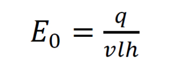
where q is laser power, v is laser velocity, l is laser thickness and h is hatch spacing.
In order to include a range of dissimilar materials in an analysis, energy density could be further normalised, through the inclusion of material-specific values for material density, heat capacity, melting temperature and bed temperature.
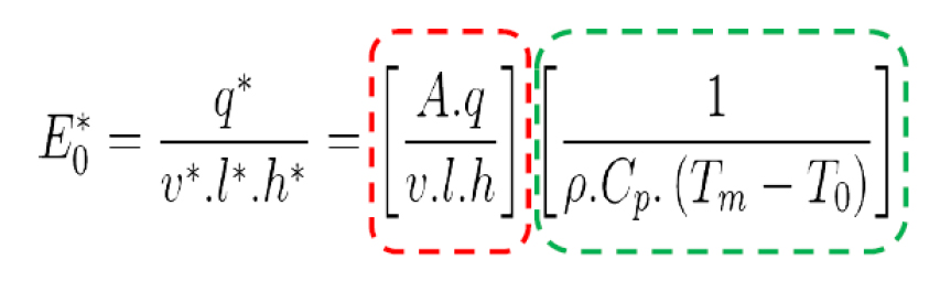
Process effects can then be considered on the basis of normalised process maps (Fig. 13). Normalised process maps were used to specify a Design of Experiment (DOE) study. Cube samples of varying size were built using a Renishaw 125 SLM system. Layer thickness was held constant at 20 µm and the variables studied were hatch spacing, laser velocity and cube size. Sections in the x-y and x-z planes were examined. Gas porosity and lack of fusion melt splashing defects were observed in both planes. Melt splashing defects were more prevalent when normalised energy density was high and were more prevalent in the x-y plane than in the x-z plane. Regression analysis showed that gas porosity increased as laser velocity decreased and hatch spacing increased. The effect of cube size was found to be insignificant. From this analysis, it was concluded that gas porosity and melt splashing can be minimised through judicious selection of processing parameters. However, for the robust SLM manufacture of IN713C components, the mechanism of crack formation still needed to be understood in order to mitigate against it.
![Fig. 13 Normalised process maps (from Meurig Thomas, Gavin Baxter and Iain Todd, Acta Materialia 108 (2016), pp. 20-35) [3]](http://www.metal-am.com/wp-content/uploads/sites/4/2016/09/13-1024x976.jpg)
In order to assess the potential contribution of chemical compositional segregation in the as-fabricated microstructure, studies were carried out using Atom Probe Tomography (ATP). The use of this characterisation technology was the University of Oxford’s contribution to the collaboration. Needle-shaped ATP specimens were removed from the built microstructure, using a Focussed Ion Beam (FIB) procedure. The atom maps created by the ATP studies showed the clustering of carbon, boron and, to some extent, zirconium at dendrite boundaries (Fig. 14).
![Fig. 14 Atom maps from LEAP analyses (Scale bar = 25 nm) [3]](http://www.metal-am.com/wp-content/uploads/sites/4/2016/09/14-1024x609.jpg)
These observations could be evidence of segregation of C, B or Zr and B and Zr are known to be deleterious for welding operations, which SLM could be deemed to be on a micro-scale. Alternatively, carbide or boride precipitates could have formed, with such precipitates potentially contributing to crack susceptibility through a high dislocation density created by their incoherence with the matrix.
In future work, line scans in ATP will be carried out over individual clusters to determine whether carbides or borides are present.
At this stage, it has been concluded that ATP is providing valuable insights into nano-scale compositional effects, but that further assessments are needed in the investigation of the crack susceptibility of IN713C. The question to be pursued is to whether minor elemental compositional adjustments could reduce crack susceptibility and make such difficult alloys processable by SLM.
Author
Dr David Whittaker is a consultant to the Powder Metallurgy industry.
Tel: +44 (0)1902 338498
Email: [email protected]
References
[1] SLM & EBM of Tungsten, J Wright, I Todd, as presented at AMPM2016, MPIF, USA
[2] Metallographic Characterization of Copper Alloys Fabricated via Selective Laser Melting, J Edgerton, as presented at AMPM2016, MPIF, USA
[3] Selective Laser Melting Of Nickel-Base Superalloys For Turbocharger Applications, C Boig, I Todd, M Burkinshaw, A London, M Moody, as presented at AMPM2016, MPIF, USA
![Fig. 1 Nuclear fusion is a promising option for generating large amounts of low carbon energy [1]](https://www.metal-am.com/wp-content/uploads/sites/4/2016/09/01-2.jpg)
LAST MONTH’S MOST-READ ARTICLES