

Additive Manufacturing for Semiconductor Capital Equipment: Unlocking critical supply chains
The global semiconductor supply chain is under immense strain as a result of geopolitical and economic factors, putting significant pressure on Semiconductor Capital Equipment (SCE) manufacturers. In this article, Emily Godsey interviews Texas A&M's Prof Alaa Elwany and Jiahui Ye, and Veeco Instruments Inc's Dr Ahmed El Desouky, to explore the benefits of metal Additive Manufacturing technologies for semiconductor manufacturing and the SCE supply chain. [First published in Metal AM Vol. 10 No. 3, Autumn 2024 | 20 minute read | View on Issuu | Download PDF]
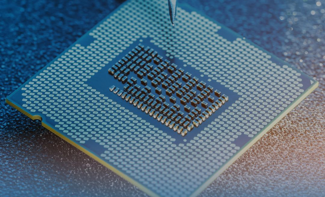
Semiconductors are critical for the fabrication of the chips and microelectronics that power nearly all modern systems, serving as the brains behind a wide range of technologies, enabling everything from smartphones to autonomous vehicles. Semiconductors are not just crucial for present-day technology; they are also foundational building blocks for future advancements in areas like AI, quantum computing, advanced robotics, and biotechnology. As these fields continue to expand, the demand for semiconductors will also rise exponentially, but meeting this demand presents challenges as more pressure is placed on supply chains.
The strain placed on the global semiconductor supply chain has been exacerbated by geopolitical factors, economic factors, and natural disruptions such as the COVID-19 pandemic. On the critical path in these chains is the production of Semiconductor Capital Equipment (SCE), the highly specialised machinery required to manufacture semiconductors. SCE involves intricate components and precision tooling, making its production costly and complex. As chip manufacturers face increasing pressure to produce more semiconductor chips, they are hampered by supply chain bottlenecks like SCE.
To overcome these challenges, SCE manufacturers are exploring the use of innovative manufacturing technologies to streamline their operations and increase supply chain flexibility. While Additive Manufacturing has, indeed, been investigated for its potential use in the semiconductor industry, much of the research to date has focused on the direct manufacture of electronic components, such as printed circuit boards or conductive materials. However, a relatively underexplored application is using AM to produce critical components for SCE.
This emerging intersection of AM and SCE holds great promise for transforming the industry. Additive Manufacturing enables rapid prototyping, reduces lead times, and allows for the creation of geometrically complex components that are well-suited to the demands of modern semiconductor manufacturing, especially for components like tooling, jigs, fixtures, and highly specialised machine parts. In particular, the ability to quickly produce custom parts for SCE may help address the production bottlenecks that are currently hindering semiconductor manufacturing at a global scale.
Dr Alaa Elwany, a professor at Texas A&M University, and PhD candidate Jiahui Ye, in collaboration with Dr Ahmed El Desouky, Director of Additive Manufacturing at Veeco Instruments Inc, are at the forefront of exploring the potential of AM in the semiconductor industry and have published on the topic [1].
Addressing challenges in semiconductor manufacturing
Semiconductor manufacturing is complex, requiring multiple classes of capital equipment to execute tasks such as gas mixing, deposition, masking, and slicing. This complexity contributes to elevated costs and extended lead times, creating challenges in maintaining supply chain resilience.
With the extensive outsourcing of semiconductor manufacturing over the past three decades, the US has faced significant supply chain disruptions, particularly during the COVID-19 pandemic. In response to these supply chain issues, the US government passed the CHIPS and Science Act of 2022, a $52.7 billion investment aimed at revitalising domestic semiconductor manufacturing capabilities and mitigating future disruptions.
“The US is working to reclaim its leadership in semiconductor manufacturing. While we have consistently led and continue to lead the world in the design and innovation of semiconductors and microelectronics, we have lost our edge in manufacturing over the past few decades,” Elwany said. “Our goal now is to rebuild our domestic capabilities in this critical industry and bring semiconductor manufacturing back to the US.
“As the US seeks to restore this leadership in semiconductor manufacturing, the need for advanced manufacturing technologies, particularly AM, becomes increasingly important,” he added.
The role of Additive Manufacturing
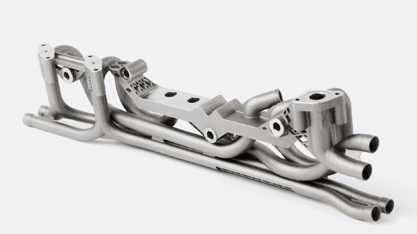
Additive Manufacturing has emerged as a critical technology to address many of the challenges faced by the semiconductor manufacturing industry as SCE manufacturers are increasingly exploring the potential of the technology to create parts that are lighter, more durable, and easier to manufacture. The ability of AM to create intricate internal structures, such as cooling channels within wafer handling systems or lattice structures within heat exchangers, opens up new possibilities for optimising the performance of SCE. In addition, AM allows for the rapid prototyping and customisation of parts, enabling manufacturers to quickly iterate on designs and bring new products to market faster.
“The use of AM in the semiconductor industry is still in its early stages,” said Ye. “Both AM and semiconductors are advanced technologies, and synergistic collaboration between the two could greatly enhance the US semiconductor supply chain.”
“The high-mix, low-volume nature of parts used in SECs makes them ideal for adopting AM,” added El Desouky. “Major SECs have complete ownership of their systems design, which is a significant advantage considering the design freedom that AM offers. This allows for optimal performance design without the boundary constraints typically encountered when designing single parts or small assemblies for AM.”
Below are some of the most promising applications of AM in the design and production of SCE.
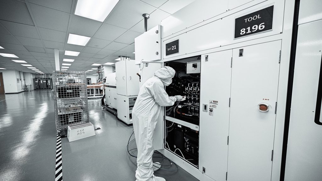
Wafer handling systems
Wafer handling systems (WHS) are critical in the semiconductor production process, as they transport, clamp, and manipulate wafers during fabrication. Wafers, thin slices of semiconductor material such as silicon, are the foundation for microelectronic devices. Throughout their production, wafers must be carefully handled to prevent contamination, ensure flatness, and maintain temperature control.
Wafer chucks – essential tools for maintaining wafer flatness and preventing contamination – are a place where AM is already making strides. Traditional wafer chucks are typically machined from metal blocks, a process that can be both time-consuming and wasteful. By contrast, AM allows for the creation of wafer chucks with conformal cooling channels, which enable more efficient heat dissipation, improve the overall performance and reduce wafer deformation.
As semiconductor devices become more complex and their processing demands increase, the need for more advanced wafer handling systems will continue to grow. AM offers a promising solution to meet these demands.
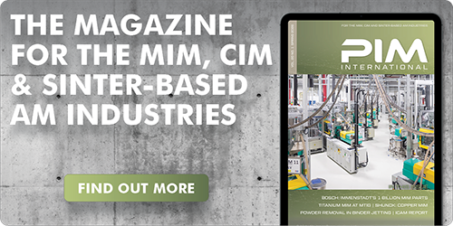
Thermal management systems
Heat exchangers play a crucial role in maintaining the efficiency of semiconductor manufacturing processes. In many semiconductor manufacturing steps, high temperatures are generated, which can negatively affect equipment performance and product quality. Effective thermal management is essential for ensuring that equipment operates within its specified temperature range, preventing overheating and ensuring the longevity of the components.
Traditional methods for fabricating heat exchangers often result in bulky and inefficient designs, but AM allows for the creation of more compact and efficient systems. By enabling the production of lattice structures and intricate internal channels, AM improves the heat transfer capabilities of these systems while also reducing their size and weight. Lattice structures, for example, offer a high surface area-to-volume ratio, which enhances heat dissipation while minimising material use.
“Next-generation heat exchangers have to be developed to support advanced SCE capable of meeting increasing demands for chips,” Ye noted.
Fluid delivery systems
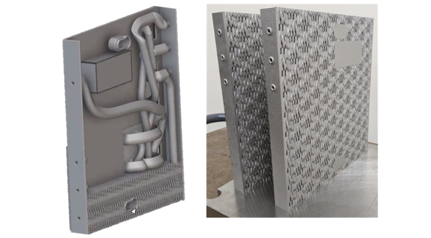
Fluid manifolds and channels are key components in gas and liquid control systems within SCE. These systems are used to transport gases and liquids to various parts of the equipment, ensuring that processes like Chemical Vapour Deposition (CVD) and plasma etching are carried out with precision. Traditionally, these parts are produced via machining and drilling, leading to bulky designs with significant pressure loss.
AM allows for optimised fluid paths and reduced pressure drops, resulting in more efficient, compact, and lightweight fluid systems. The ability to design fluid channels with smooth transitions and curved paths, rather than the right-angle bends common in traditional designs, reduces turbulence and improves flow efficiency. This is particularly important in applications such as modular gas delivery systems, where efficiency and customisation are critical. Additionally, AM designs enable the creation of more complex, compact structures, providing significant footprint savings. This is particularly important in clean rooms, where every square foot saved can lead to substantial long-term cost benefits.
Precision flexure stages
Plexure stages, which provide precise movement control for components in semiconductor manufacturing, have also benefitted from AM. In processes such as lithography, where precise alignment of masks and wafers is essential for creating integrated circuits, flexure stages are used to position components with sub-micron accuracy. AM enables the creation of complex flexure designs with integrated joints and monolithic structures, features not achievable via the traditionally used subtractive manufacturing methods.
Challenges and opportunities
While the benefits of adopting AM in semiconductor manufacturing are clear, several challenges remain that need to be addressed before AM can be fully integrated into SCE production.
Material selection
The range of materials suitable for AM remains somewhat limited, particularly for high-performance components. For example, copper, which is widely used in semiconductor equipment due to its thermal and electrical conductivity, presents challenges in AM processing because of its low energy absorption.
Additionally, commonly used AM alloys may contain elements that negatively interact with process gases, complicating deposition processes. Developing new materials specifically designed for use in semiconductor equipment will be crucial in overcoming this challenge.

Process optimisation
Achieving the high levels of precision required in semiconductor manufacturing often demands post-processing techniques, such as surface finishing and machining, to enhance the quality of additively manufactured parts. Further research into optimising AM processes and reducing defects like porosity will be essential for improving part reliability.
The high variability in the surface finish, porosity, and mechanical properties of AM parts can affect the repeatability of material deposition processes. Although the semiconductor industry may not be as heavily regulated as others, it emphasises ‘copy-exact’ standards, meaning part-to-part repeatability is crucial throughout the AM and subsequent post-process chain.
Quality Control
Additionally, the qualification and certification of AM components to ensure that they meet design requirements present significant barriers. SCE must meet extremely tight tolerances and high-performance criteria, often under harsh operating conditions. This makes the qualification process for AM components particularly challenging, as they must demonstrate consistent quality, thermal and mechanical resilience, and long-term repeatability under high temperatures and continuous use. AM process modelling and simulation will play a vital role in optimising designs and build parameters to minimise distortion and ensure consistent part-to-part repeatability. In addition, advanced quality control methods, including real-time monitoring, high-throughput non-destructive evaluation techniques, and machine learning-based inspection, are being developed to ensure that AM parts meet industry standards.
Collaboration is key
For AM to reach its full potential in the semiconductor sector – including the production of SCE – this collaboration must be more structured and involve mechanisms like public-private partnerships. These partnerships should bring together diverse stakeholders from across the innovation ecosystem, including government funding agencies, academia, small startups, and large industry players. By pooling resources and expertise, these partnerships can tackle the technical and regulatory challenges that have slowed the adoption of AM in semiconductor capital equipment production.
“AM technologies have made significant strides in heavily regulated industries such as medical and aerospace,” stated Dr Ahmed El Desouky. “However, adoption in the semiconductor industry is still in its early stages due to questions around chemical stability and cleanliness. While we are currently able to address many of these questions, we are barely scratching the surface. Collaboration between manufacturers and academia will unlock numerous opportunities for the manufacturing of complex assemblies, ultimately improving productivity and cost of ownership.”
Dr Elwany continued, “Public-private partnerships are important when we want to de-risk the adoption of advanced technologies like AM, especially in its application to complex industries such as semiconductor manufacturing. Success stories can be seen in the Manufacturing USA institutes, where government, industry, and academia collaborate to accelerate manufacturing innovation. We need similar efforts specifically geared toward the use of AM for the production of semiconductor capital equipment.”
Outlook and conclusion
AM represents a significant opportunity for the semiconductor industry to overcome current challenges and future-proof its production processes. By leveraging AM, semiconductor manufacturers can enhance the design, performance, and efficiency of their capital equipment while strengthening the resilience of the global supply chain.
While there are barriers to overcome that are currently halting the widespread adoption of AM in the semiconductor industry, further research from public-private partnerships can position Additive Manufacturing technology as a critical tool in strengthening the semiconductor supply chain.
As Elwany concluded, “AM holds the potential to help the US reclaim its position as a global leader in semiconductor manufacturing and strengthen its domestic supply chain, with direct impacts on the nation’s economic prosperity and national security.”
Author
Emily Godsey
Texas A&M Engineering
www.tamu.edu
Contact
Prof Alaa Elwany
ASME Foundation Swanson Fellow
College of Engineering Eugene Webb Faculty Fellow
Director – Texas A&M Metal Additive Manufacturing Research Laboratory (AMTex)
[email protected]
www.tamu.edu
References
[1] Jiahui Ye, Ahmed El Desouky and Alaa Elwany, On the applications of additive manufacturing in semiconductor manufacturing equipment, Journal of Manufacturing Processes, Volume 124, 30 August 2024, 1065-1079
LAST MONTH’S MOST-READ ARTICLES