

Simple and standardised X-ray CT testing in metal Additive Manufacturing
X-ray Computed Tomography (CT), also widely known as MicroCT, is a proven method for not only checking the structural integrity of additively manufactured (AM) parts - for example for unwanted porosity - but also for checking a build’s dimensional accuracy. The main advantage of the technique is, of course, the non-destructive nature of the assessment; however, there are also many misunderstandings about the capabilities and complexity of the technology. Prof Anton du Plessis and Dr Jess M Waller review the application of CT testing in relation to metal AM and highlight the advantages of a move towards standardised test methods. [First published in Metal AM Vol. 4 No. 4, Winter 2018 | 20 minute read | View on Issuu | Download PDF]
Most metal Additive Manufacturing engineers have heard of CT scanning and seen exciting 3D X-ray images. Some have even used the technique, and some use it extensively. However, whenever the topic is mentioned, a combination of the following is often heard from AM engineers:
- It costs too much
- It takes too long
- It’s too complicated
- Does it really help?
- It’s too variable in quality
- It’s too variable in cost and time
- It’s too ‘fancy’ and not for production
- Which defects matter or are rejectable?
- What is the critical initial flaw size for metal AM parts that must be reliably detected?
- How reliable is the technique for detecting deeply embedded flaws?
- I’ve characterised the defect state, i.e., defect sizes, types, orientations and distributions, but what about microstructure-dominated failure mechanisms?
- I’ve heat treated or subjected my part to Hot Isostatic Pressing, thus closing the pores as revealed by before and after CT. Do I still need to be worried?
All of the above leads to one unfortunate result: engineers are not using the awesome power of CT to improve Additive Manufacturing, despite its availability. First, take a step back and look again at the first few comments in the list above. It sounds very much like a description of metal Additive Manufacturing you may have heard a few years ago, doesn’t it? The exciting news is that all the above issues are now either resolved or significant progress has been made towards resolving them, and microCT is taking its place as the method of choice to inspect AM parts. This article explains why and how, whilst also reviewing current CT standardisation efforts and resources.

How does X-ray CT work?
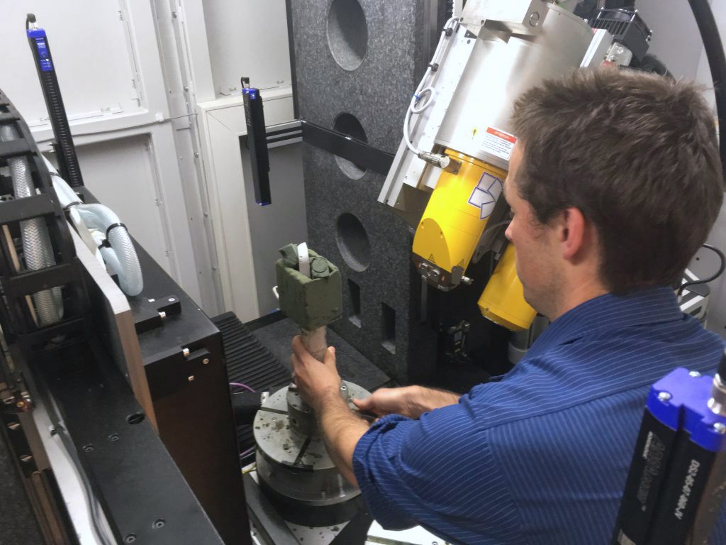
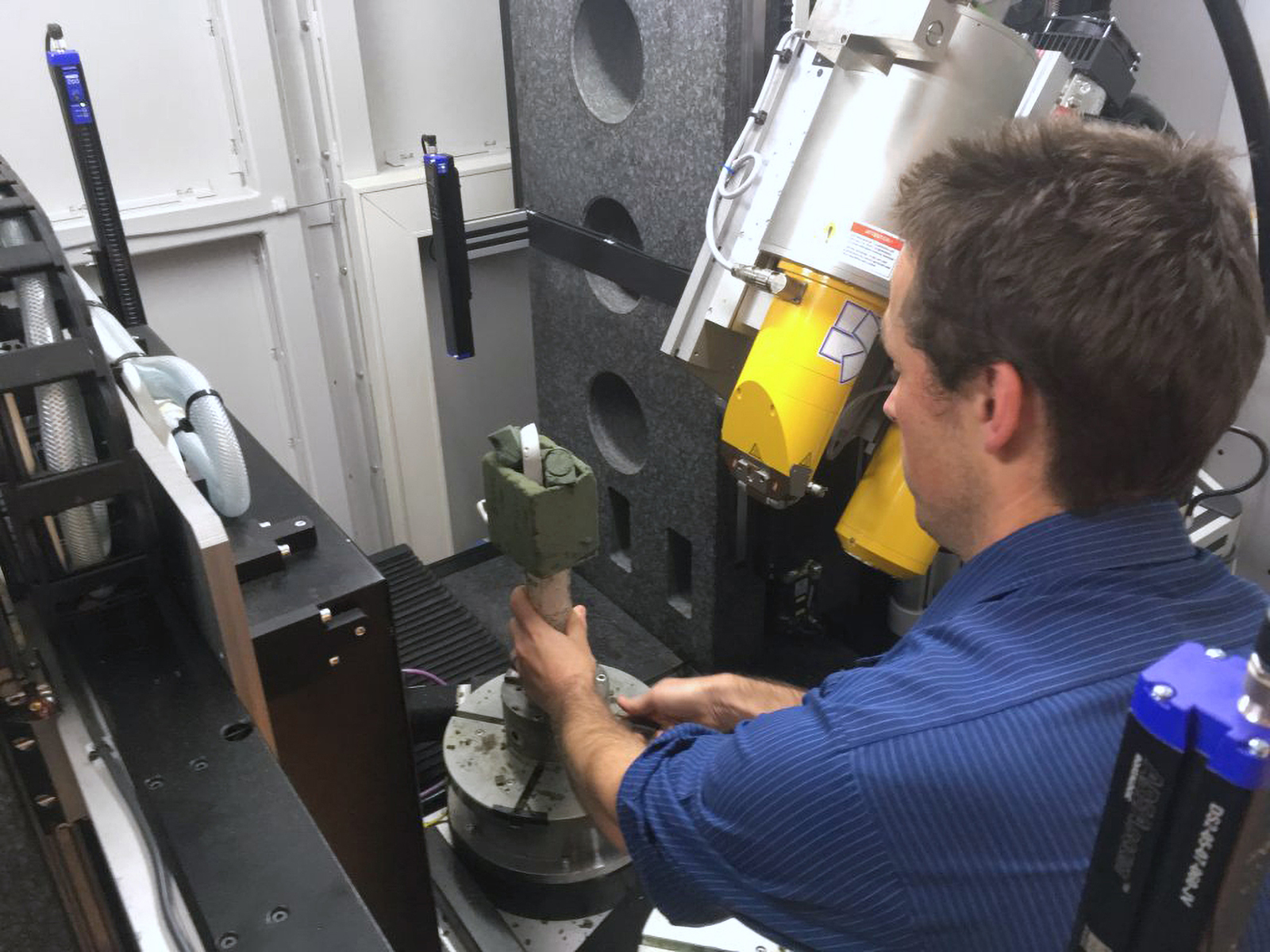
Fig. 1 shows a sample being loaded in an industrial X-ray CT system. When X-rays are projected through and around a sample, they form a ‘shadow’ image, or X-ray image, of the object on a digital detector. This is essentially the same as a doctor’s office X-ray and, for industrial parts, is known as digital radiography. This method is very useful to check for unexpected features: cracks, pores or inclusions. While detection of these features may not necessarily be grounds for part rejection, their detection may warrant archiving as a quality record, or review by a material review board or cognizant engineering organization to determine final disposition of the part.
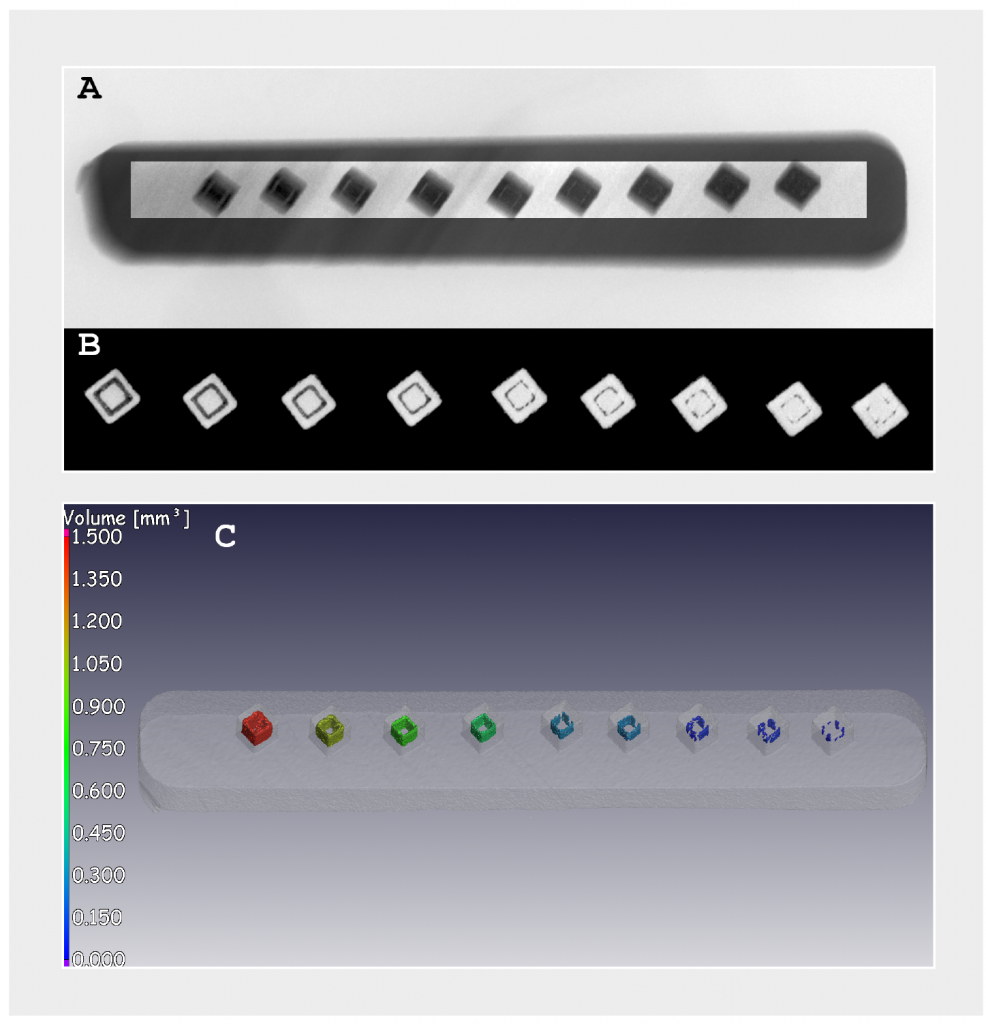
However, radiography provides limited contrast and a strictly two dimensional view. By recording images from many angles as the object rotates, a CT scan is recorded and full 3D data are generated. After recording the images, a back-projection algorithm calculates the X-ray density at each point in the object. This results in much higher contrast images than radiographs (but many more of them!), with full 3D information – location, width, pore to surface distance, etc., as demonstrated in Fig. 2. In high value parts subject to fracture critical requirements, more rigorous and comprehensive CT analysis may be required, including characterisation of flaw shape, orientation relative to principal stresses, nearest neighbor pore to pore distances, and determination of the probability of detection (POD) for a given flaw size [1,2,3]. In advanced CT applications, extreme value statistics can be used to predict the fatigue strength and service life of an object by describing the defect population and determining the most critical defect distribution. This, in turn, can simplify the CT scan by determining the minimum volume that needs to be inspected to ensure the required CT precision [4]. A typical X-ray image is shown in Fig. 2(a) with a rectangular area of interest contrast-enhanced to show the presence of intentionally designed cavities (white areas inside darker area). The subsequent full microCT scan in Fig. 2(b) shows in a slice image the same cavities in much higher contrast (with inverted contrast – pore spaces are black and material is white). Fig. 2(c) shows a transparent 3D rendering of the square pore spaces, with colour coding based on volume (processed microCT data).
Computed tomography is known by many names and can be used in different ways, which might make it seem complicated. X-ray CT, microCT, nanoCT, microtomography, CT scanning, X-ray microscopy; all are effectively the same technique. As with all technologies, some types of equipment are suited to specific types of samples while others are better suited for other types of samples. However, the major point often overlooked is the processing of the 3D data – the handling, processing and analysis of 3D data sets was until recently the biggest hurdle to use the technique effectively. With today’s high-spec computing workstations with multiple CPUs, high-end graphics cards, solid state drives and large amounts of RAM available, the analysis of large amounts of CT data becomes more efficient and much more useful, especially when using dedicated software for the purpose. Examples in this article are produced using Volume Graphics VGSTUDIO Max 3.2 with workstations using dual-core CPUs, NVidia graphics cards and 64–128 GB RAM. Scans here reported are performed at the Stellenbosch CT facility [5] and in all cases can be performed with a typical commercial microCT system with microfocus X-ray source capability up to 225 kV. Higher voltage systems and macro¬scale CT systems are also available and applicable for larger and denser AM parts (where microCT starts to be limited, as will be discussed below), but these are less widely available than microCT. For many applications, it is cost-effective to make use of the growing number of microCT service providers available globally.

What are the technology’s uses in Additive Manufacturing?
MicroCT has proven to be useful for checking the structural integrity of AM parts, i.e., to check for unwanted porosity or other flaws introduced during build. It is also used to check the dimensional accuracy, as parts may warp or otherwise build inaccurately – and microCT is the only way to create a full 3D model of a complex part with hidden or challenging geometries [1,6,7,8]. The need to develop new CT standards for measurement of internal features in AM parts using existing CT standards on a basis (E1570 [9], E1695 [10], VDI/VDE 2630 [11], WK61161 [12] and WK61974 [13]) was recently identified as a key NDE standardisation need in the United States [14]. Namely, current CT metrology state-of-the-art needs to be tailored to evolving AM part inspection requirements, including measurement of small or intricate AM features, and verification of the form and fit of lattice structures [14]. In its current form, the main advantage of the CT technique is the non-destructive nature of the assessment: this means that the dimensional accuracy and internal integrity can be assessed and the part approved or rejected based on pre-determined criteria [3], depending on the criticality of the application, i.e., as a quality control tool [15,16,17]. Despite many newer applications of the technology, this is still the most valuable application of microCT in AM. It is clear that this will become indispensable as AM moves more and more towards production and such quality control becomes essential, especially for high-value and structurally critical parts such as those for medical or aerospace applications.
What are the limits?
Not everything can be scanned, much like not everything can be additively manufactured. The physical size limits are typically based on the size of the CT cabinet; however, this is not the most critical consideration. The major point is that as the sample gets bigger, the resolution gets poorer due to field-of-view limits, and with this comes increasing likelihood of image artefacts such as beam hardening due to the larger amount of material that needs to be penetrated by the X-ray beam. Due to complex parts with varying densities and the fact that a cone beam geometry is often used, some image artefacts are almost always present in obtained images. Fan beam geometries are sometimes used to eliminate artefacts but these scans take more time to acquire, and therefore are not well suited to high-throughput inspections. In general, the smaller the sample, the better the results due to both above reasons – better resolution and fewer artefacts. There is no hard rule for ‘high-quality data’ vs ‘poor-quality data’ and, in reality, anything can be scanned – the results simply degrade as the part gets bigger.
Choice of resolution is one of the misunderstandings of the technique in general, as the same part can be scanned at either 30 or 100 µm, for example, but the detail seen at 30 vs 100 µm is not the same. Smaller pores are visible at higher resolution, which can make it seem like the part has more porosity, but this is not the case necessarily. For one-to-one comparisons, one must compare scans of similar parts at the same resolution, ideally with the same scanner settings and the same contrast, and obviously with the same image analysis method. This is exactly where standardised workflows, which have recently been introduced in our group at Stellenbosch University, can support the wider and improved adoption of the technique for Additive Manufacturing.
Besides resolution vs sample size, some material types are simply too radiodense to scan, and this ‘impossibility’ is again not a hard threshold, as the quality of the scan data degrades as the part becomes larger. In general, steel (which is strongly X-ray absorbing due to heavier atomic mass atoms) is challenging to scan, and therefore microCT using typical laboratory CT systems is better suited to lighter metals. When steel parts are small (solid parts up to 8 mm, or multiple wall thickness up to 8 mm total in line with the X-ray), the method works reasonably well using typical microfocus sources up to 225 kV. For larger steel parts or heavier metals, higher voltage systems may be the only solution. Otherwise, low-quality images may be sufficient to get an idea of structural integrity, without detailed quantitative evaluation. On the other hand, Ti-6Al-4V parts up to 200 mm can be scanned on 225 kV systems with full quantitative evaluations, to give an idea of the sample sizes possible. All examples shown in this article are for Ti-6Al-4V.
As shown above, the scan quality is influenced by resolution, part size and material type, all affecting the presence of image artefacts and affecting the detectability of small flaws. Of course, many other factors also affect the quality of the obtained images – increasing image averaging reduces inherent noise, but makes scan times longer. Scanning multiple samples together is sometimes possible, but puts a limit on the best possible resolution that can be obtained. Using shorter image acquisitions and less averaging allows much faster throughput but increased noise in images. Despite all of these complex considerations, there are some general guidelines or best-practice methods that can be followed [9,18]. The acquisition of good images and subsequent analysis for a specific purpose might sometimes seem like an art more than a science, understood only by skilled experts. This brings us to an important point: if you scan the same part at different service facilities, do you get the same answer? Up to now, this was not the case. Luckily, standardisation has now arrived in this industry, despite the above challenges.
In addition to part complexity and size, which directly affect CT inspectability, other part characteristics may place added demands on the requisite precision and rigour of the CT technique used. The combined effect of these characteristics is denoted ‘AM risk’ [16]. Simply put, high AM risk parts require the use of highly reliable and precise CT techniques, possibly including other NDE methods to ensure complete coverage of all part surfaces and volumes. Part characteristics contributing to ‘AM risk’ ranked in order of importance are 1) the inability to perform adequate proof testing based on the anticipated design stress state, 2) the inability to remove the as build surface from all fatigue-critical surfaces, 3) the inability to access and improve surfaces interfacing any sacrificial supports, 4) the presence of thin (< 1 mm) walls and protrusions, and 5) the presence of critical regions requiring sacrificial supports. In such cases, the onus placed on CT can be extreme, and can result in situations where it is difficult, if not impossible to inspect a part by CT or other means.
Lastly, since location-dependent properties in as-built AM parts are affected by complex interactions between defect-dominated and microstructure-dominated failure mechanisms [19], the interaction between defects and microstructure needs to be better understood. Until this understanding matures, in addition to characterising the defect state as revealed by CT or other NDE, the need to characterise the microstructure as revealed by metallography, fractography, etc., is highlighted if Additive Manufacturing parts with desired location-specific properties are to be produced.
Standardised CT test methods
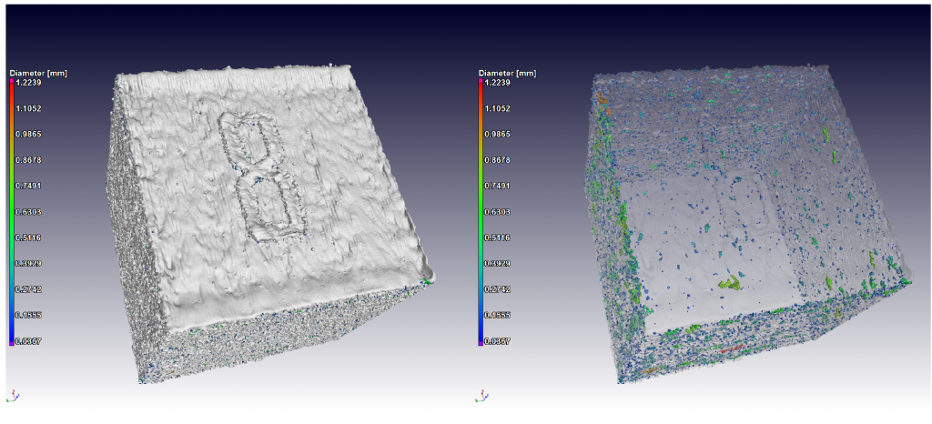
Standardised test methods were proposed recently and implemented in a round robin test [20-26]. These methods simplify the workflow, with the ultimate aim of improving the quality of AM processes and parts. The first standard test method involves a simple 10 mm cube as the coupon sample. Such a small coupon sample is already used in many optimisation processes for AM and should therefore be simple to incorporate in existing optimisation workflows. The idea is that, for a given sample size (i.e., 10 mm), a fixed resolution can be used for the scan. Coupled with some general guidelines on scan parameters, a precise image analysis workflow can be generated where human input is minimal, resulting in a standard test method. For this 10 mm cube, a simplified workflow results in a detailed porosity analysis [26]. This result is not only a quantitative evaluation of the porosity, which can act as feedback for process optimisation, but also the 3D distribution, location and shape of pores can assist in understanding the root cause of problems in the manufacturing process and, therefore, allowing much faster correction of the real problem compared to past trial and error methods. In the example shown in Fig. 3 there is a contour scanning error, a reasonably well-known in-process laser or electron beam scanning error, which can be fixed by reducing the space between contouring and hatch scan lines. This type of information can therefore be used to optimise the process for each new type of powder or process, qualify a process for production, or check process parameters on a regular basis to ensure quality builds. It is important to realise that the analysis workflow is simplified and semi-automatic, removing almost all possible human bias from the process.
The next standardised method involves using the same 10 mm cube (no additional scan is required) and measuring the total volume accurately using microCT data, then measuring the mass of the cube, thereby obtaining a mean CT-density value. While the Archimedes density measurement method is well known, this CT-density method holds some advantages, especially for typical as-built AM surfaces, which might trap air bubbles in a water-Archimedes test, or when open pores may result in water filling large internal cavities, resulting in improper Archimedes measurements. It is also very simple and not much effort when the CT data are already available. The added benefit is that, when an irregular density value is found, the images may help to understand why this is the case and therefore better understand the problem. This standardised image analysis workflow, which is described in detail in [21], is also entirely automated.
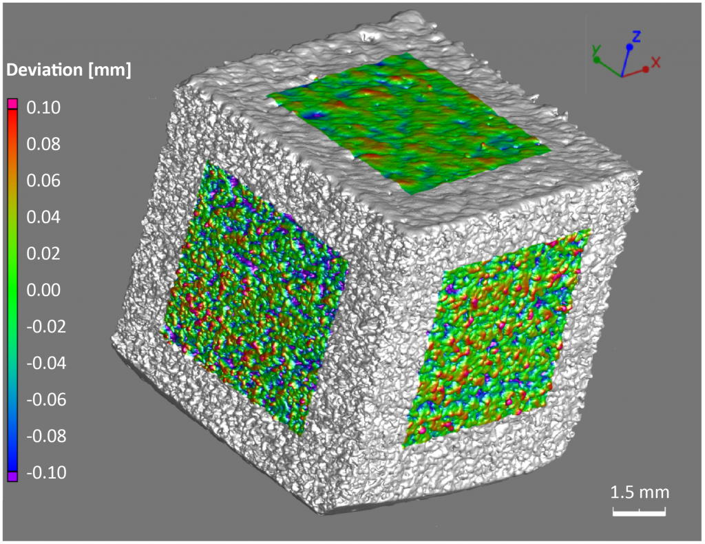
Evaluation of surface roughness is also possible using microCT data, using the same 10 mm cube. A standard workflow [22] was proposed for this purpose and an example is shown in Fig. 4, which shows the top surface is much smoother than the vertical surfaces, as expected for Laser-Beam Powder Bed Fusion parts. The colour-map shows deviation of the actual surface from the mean plane representing the surface. Output of the deviation values allows calculation of an Sa value, which expresses, as an absolute value, the difference in height of each point compared to the arithmetical mean height of a surface. The main benefit of this process is the simplicity and the possibility to assess build quality in multiple ways (porosity content, density, and roughness) using only one scan of a coupon sample. The use of a standard workflow also ensures high reproducibility.
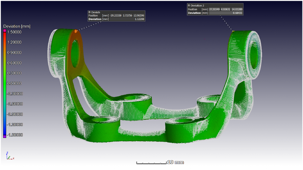
Besides using small coupon samples for optimising and characterising the general build quality, quality inspection of real (typically complex-shaped) parts is equally important. Here we demonstrate a topology optimised bracket, which was used in a round robin production test, i.e., the same set of parts were produced in different LB-PBF systems and the resulting parts all analysed using the standardised microCT workflows [20,23]. The result shown in Fig. 5 is an example of one such bracket compared to its design; in this case, warping of the vertical sections inwards by more than 1 mm is seen on the left side.
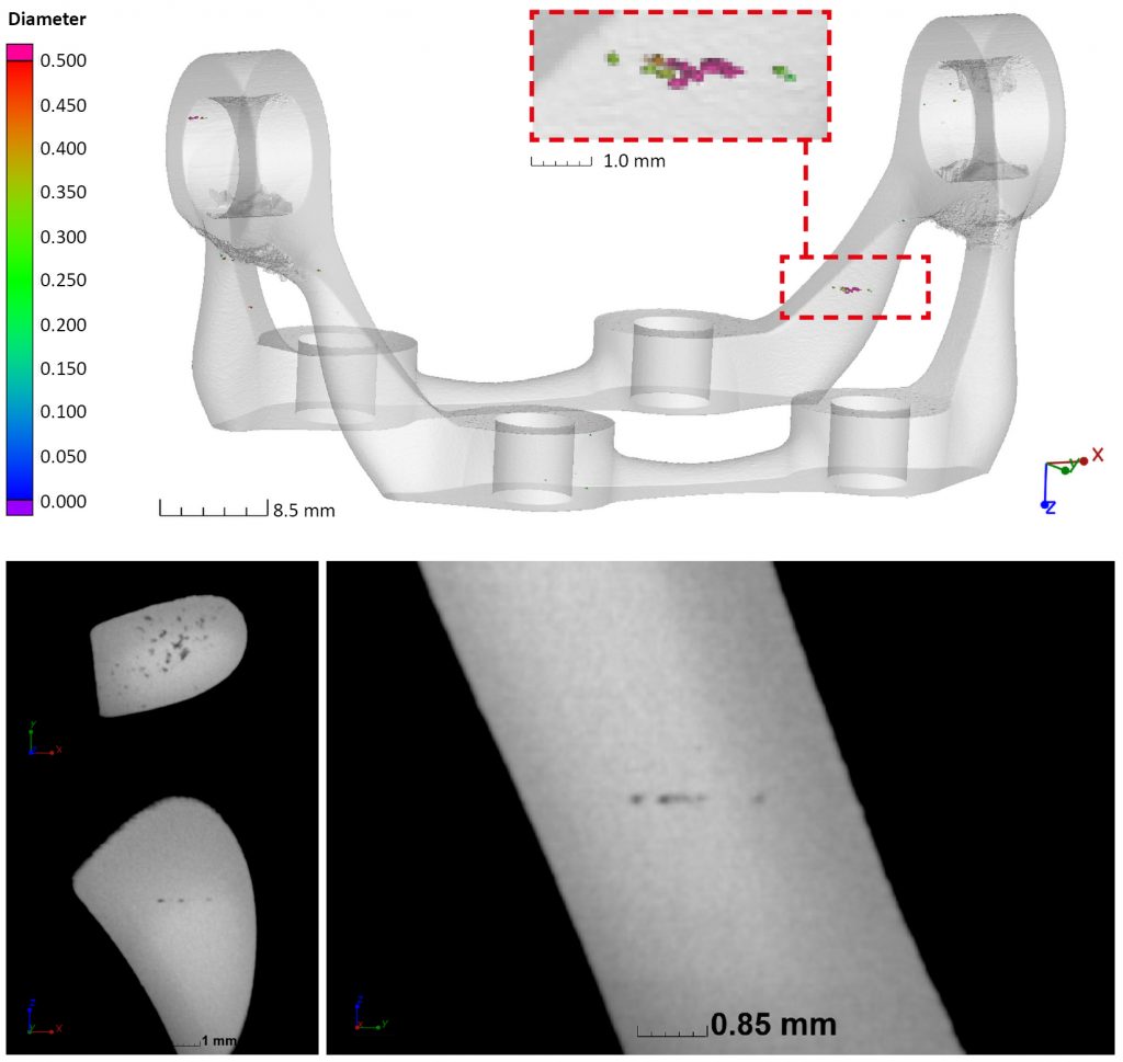
Shown in Fig. 6 is an example of unexpected porosity found in a section of a sample as shown in various microCT views. Besides unexpected porosity, which can have several causes or manifestations (gas porosity, keyhole porosity, chained porosity, surface breaking porosity, skipped layers, etc.), microCT can help to identify other issues in AM parts as part of a quality inspection [1,7,8]:
- Lack of fusion (lack of penetration between a deposited layer and the previously deposited substrate)
- Inclusions (dense particles, e.g., from contamination of the powder or build chamber, or segregation of species upon cooling from the melt)
- Unconsolidated or trapped powder (unfused feedstock stuck inside lattice structures or internal cavities inside complex parts)
- Cracks (hot tear, cold cracking, delamination)
- Surface flaws (notches, stair stepping, spatter, sag, balling, worm track, contour separation)
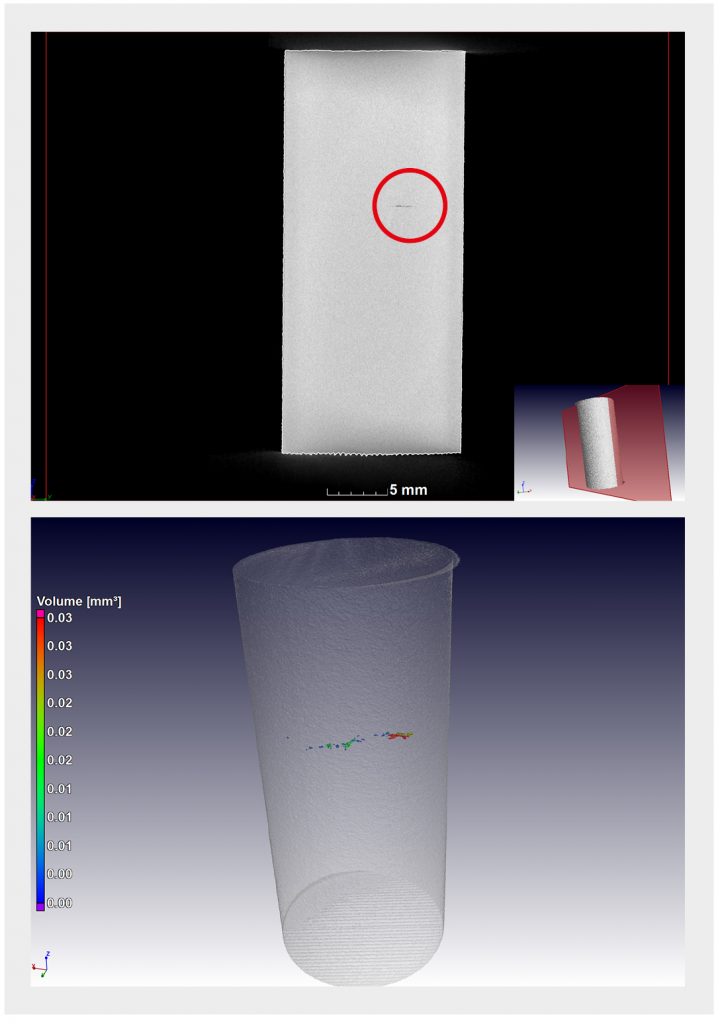
As mentioned in the previous section, resolution is limited by sample size. Therefore, a large part cannot be evaluated to the same detailed resolution as a smaller part. One way to help overcome this problem is to also scan a witness specimen, in this case a small vertically-built cylinder, built alongside the complex part. This allows high-resolution scanning of the witness specimen, and an assessment of the general quality of the build. In addition, since the witness specimen is a fixed dimension, CT scan parameters and the resulting workflow can be refined and standardised across different AM processing platforms, or for different pieces of equipment within a given AM processing platform.
The logic for the witness specimen is that many types of flaws may occur across the entire build – one such flaw is a stop-start flaw, which is a layered flaw induced when the system stops and is restarted. This was intentionally induced in the example shown in Fig. 7.
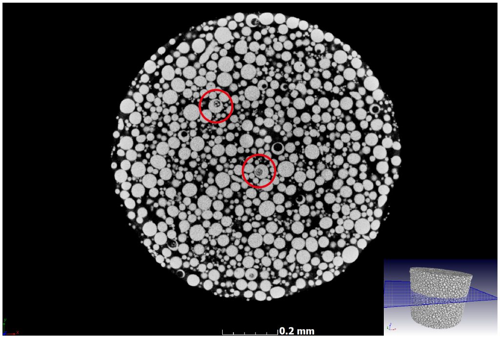
The above-mentioned standard workflows for porosity content, density, and roughness are supplemented by a standard workflow for analysing metal powder by high-resolution microCT (e.g., from different suppliers). The standard workflow is described in [24], with an interesting result from one specific Ti-6Al-4V powder batch shown in Fig. 8. In this case the gas atomised powder is mostly spherical (round in the slice image), with some gas porosity inside particles as shown by the round black areas. What is interesting here is the presence of fine powders trapped inside cavities inside particles, indicated in two cases by red circles. This indicates the presence of ‘powder inside powder’, i.e., fine powders trapped inside pores in larger powder particles! There is simply no other way to see this than by microCT.
The standardised methods discussed above are useful because the fixed sample sizes (a 10 mm cube, a vertically-built witness cylinder, or a fixed tube diameter of metal powder) allow a uniform CT scan resolution, which effectively allows simplified and exact scanning and image analysis steps to be followed. Additionally, the image analysis steps in the workflows are mostly automated, minimising the influence of human bias or image analysis errors in the process. The end result is a simpler and more easily reproducible method, even for less experienced analysts. When using a service provider for this analysis, the transparency in the workflow allows a simpler and lower price structure. This addresses the issue of ‘CT takes too long’ and ‘CT costs too much’, while also ensuring useful and reproducible results, not simply ‘fancy’ results.
The cube porosity analysis (scan plus analysis, entire job) takes a maximum of four hours, with typical service providers charging $150 per hour, to give an idea of an approximate cost.
Conclusion
It is clear that microCT is a powerful ally for Additive Manufacturing. By using the power of microCT, not only can quality inspections improve the success rate of critical parts, manufacturing processes can be improved and problems eliminated sooner in the fastest possible time, even during powder feedstock screening and acceptance.
While the detection of unwanted porosities or inconsistencies using microCT has been well known for some time, its wider use has been lagging in this industry due to costs and quality variances, which are not always transparent or easily understood. With the incorporation of standard methods and best-practice workflows, easier usage and improved interpretation of CT results is made possible.
Not mentioned in this article are the multitude of other applications and emerging methods of using microCT to the benefit of AM research and eventually industrial production: these are discussed in detail in a recent comprehensive review article [25]. The use of the standardised methods in the round robin production test is also reported in detail in [20]. Descriptions of the standardised methods and videos showing every step are available at www.protocols.io.
It is clear that metal Additive Manufacturing is an immensely promising field, and this will be amplified even more once microCT is adopted and widely used as the leading test method for quality inspection and process optimisation. There is a bright and exciting future for both these technologies.
Application of the described workflows will also help to surmount some of the more difficult technological hurdles that remain. Those hurdles relate to knowledge of the critical initial flaw size, detection of deeply embedded flaws, reliability of detection, effect-of-defect (including understanding effect of closed porosity after post-processing), and developing a clearer understanding of the role of defect-dominated versus microstructure-dominated failure mechanisms. However, to tackle these more entrenched issues, part variability due to differences in porosity, density, surface roughness, and feedstock must be controlled first. The workflows described herein are central to that task.
Authors
Anton du Plessis
Associate Professor
Stellenbosch University Room 1046,
Paul Sauer Building,
Bosman str,
Stellenbosch 7600 South Africa
Tel: +27 21 808 9389
Email: [email protected]
www.sun.ac.za/ctscanner
Jess M Waller
Materials Scientist/HX5 Teammate
NASA-JSC White Sands Test Facility
Laboratories Department
Las Cruces, NM 88004, United States
Email: [email protected]
Resources and references
Standardised method descriptions and workflow videos are available on protocols.io: www.protocols.io/ researchers/anton-du-plessis/protocols. The review paper is open access and available here: www.liebertpub. com/doi/abs/10.1089/3dp.2018.0060
[1] B. Dutton, W. Vesga, J., Waller, S. James, and M. Seifi, “Additive Manufacturing Defect Formation and NDE Detectability,” ASTM Symposium on Structural Integrity of Additive Manufactured Parts, Washington, DC, Nov. 6-8, 2018, ASTM STP 1620, M. Seifi and N. Shamsaei, Eds., ASTM International, West Conshohocken, PA, 2018 (in review).
[2] J. Madison, L. Swiler, O. Underwood, B. Boyce, B. Jared, J. Rodelas, B. Salzbrenner, “Identification of Defect Signatures in an Additively Manufactured Precipitation-Hardened Stainless Steel,” TMS 2017, SAND2017-2233C, Sandia Natl. Laboratories, Albuquerque, NM.
[3] NASA-STD-5009A, “Nondestructive Evaluation Requirements for Fracture-Critical Metallic Components,” June 19, 2018, available from the NASA Technical Standards System at the NASA website www.standards.nasa.gov.
[4] S. Romano, A. Brandão, J. Gumpinger, M. Gschweitl, S. Beretta, “Qualification of AM parts: Extreme value statistics applied to tomographic measurements,” Mater. Des. 131. 32–48 (2017).
[5] A. du Plessis, S.G. le Roux, A. Guelpa, The CT Scanner Facility at Stellenbosch University: An open access X-ray computed tomography laboratory, Nucl. Instruments Methods Phys. Res. Sect. B Beam Interact. with Mater. Atoms. 384 (2016) 42–49. doi:10.1016/J. NIMB.2016.08.005.
[6] E. Todorov, R. Spencer, S. Gleeson, M. Jamshidinia and S. M. K. Ewi, “Nondestructive Evaluation (NDE) of Complex Metallic Additive Manufactured (AM) Structures,” America Makes: National Additive Manufacturing Innovation Institute (NAMII), AFRL-RX-WP-TR-2014-0162, Wright-Patterson Air Force Base, Ohio, June 2014.
[7] ASTM WK47031, draft “Standard Guide for Nondestructive Testing of Metal Aerospace Additive Manufactured Parts After Build,” Technical Point of Contact: Jess Waller, ASTM International, West Conshohocken, PA, in ballot, https://www.astm.org/WorkItems/WK47031.htm.
[8] ISO/ASTM DTR 52905 (ASTM F42), “Additive manufacturing — General principles — Non-destructive testing of additive manufactured products,” draft standard, Convener: Ben Dutton.
[9] ASTM E1570-11, “Standard Practice for Computed Tomographic (CT) Examination,” ASTM International, West Conshohocken, PA (2011).
[10] ASTM E1695-95(2013), “Standard Test Method for Measurement of Computed Tomography (CT) System Performance,” ASTM International, West Conshohocken, PA (2013).
[11] VDI-Standard: “Computed tomography in dimensional metrology: measurement procedure and comparability,” VDI/VDE 2630 Blatt 1.4, The Association of German Engineers, June 2010.
[12] ASTM WK61161, draft “Practice for Volumetric Computed Tomographic (CT) Examination Using Digital Detector Arrays,” Technical Point of Contact: Trey Gordon, ASTM International, West Conshohocken, PA, in preparation, https://www.astm.org/DATABASE.CART/WORKITEMS/WK61161.htm.
[13] ASTM WK61974, draft “Practice for characterization of computed tomography systems for dimensional measurement,” Technical Point of Contact: Thomas Wentzel, ASTM International, West Conshohocken, PA, in preparation, https://www.astm.org/DATABASE.CART/WORKITEMS/WK61974.htm.
[14] Additive Manufacturing Standardization Collaborative (AMSC), “Standardization Roadmap for Additive Manufacturing,” Version 2.0, ANSI and NDCMM/America Makes, June 2018, https://www.americamakes.us/america-makes-ansi-publish-version-2-0-standardization-roadmap-additive-manufacturing/.
[15] R. Russell, D. Wells, J. Waller, B. Poorganji, E. Ott, T. Nakagawa, J. Sandoval, N. Shamsaei, and M. Seifi, “Qualification and Certification of Metal Additive Manufactured Hardware for Aerospace Applications,” Chapter 3, in Additive Manufacturing for the Aerospace Industry, Boyer and Froes, Eds., Elsevier, 2019 (in press).
[16] D. N. Wells, “Standard for Additively Manufactured Spaceflight Hardware by Laser Powder Bed Fusion in Metals,” MSFC-STD-3716, NASA Marshall Spaceflight Center, Huntsville, AL, October 18, 2017.
[17] D. N. Wells, “Specification for Control and Qualification of Laser Power Bed Fusion Metallurgical Processes,” MSFC-SPEC-3717, NASA Marshall Spaceflight Center, Huntsville, AL, October 18, 2017
[18] A. du Plessis, C. Broeckhoven, A. Guelpa, S.G. le Roux, Laboratory x-ray micro-computed tomography: A user guideline for biological samples, Gigascience. (2017). doi:10.1093/ gigascience/gix027.
[19] M. Seifi, A. Salem, J. Beuth, O. Harrysson, and J.J. Lewandowski, “Overview of Materials Qualification Needs for Metal Additive Manufacturing,” Journal of the Materials, Minerals, Metals & Materials Society (JOM), 68, 747 (2016).
[20] A. du Plessis, S.G. le Roux, Standardised X-ray tomography testing of additively manufactured parts: a round robin test, Addit. Manuf. (2018). doi:10.1016/J.ADDMA.2018.09.014.
[21] A. du Plessis, P. Sperling, A. Beerlink, L. Tshabalala, S. Hoosain, N. Mathe, G. Stephan, MethodsX Standard method for microCT-based Additive Manufacturing quality control 1 : Porosity analysis, MethodsX. 5 (2018) 1102–1110. doi:10.1016/j. mex.2018.09.005.
[22] A. du Plessis, P. Sperling, A. Beerlink, L. Tshabalala, S. Hoosain, N. Mathe, G. Stephan, MethodsX Standard method for microCT-based Additive Manufacturing quality control 2 : Density measurement, MethodsX. 5 (2018) 1117–1123. doi:10.1016/j. mex.2018.09.006.
[23] A. du Plessis, P. Sperling, A. Beerlink, O. Kruger, L. Tshabalala, S. Hoosain, S.G. le Roux, Standard method for microCT-based Additive Manufacturing quality control 3: Surface roughness, MethodsX. 5 (2018) 1111–1116. doi:10.1016/j. mex.2018.09.006.
[24] A. du Plessis, P. Sperling, A. Beerlink, W. du Preez, S.G. le Roux, Standard method for microCT-based Additive Manufacturing quality control 4: Metal powder analysis, MethodsX. 5 (2018) 1336–1345. doi:10.1016/j. mex.2018.09.006.
[25] A. du Plessis, Standard method for microCT-based Additive Manufacturing quality control 5: witness specimen, Protocols.Io. (2018). https://www.protocols.io/view/ standard-method-for-microct-based-additive-manufac-sbzeap6.
[26] A. du Plessis, I. Yadroitsev, I. Yadroitsava, S.G. Le Roux, X-Ray Microcomputed Tomography in Additive Manufacturing: A Review of the Current Technology and Applications, 3D Print. Addit. Manuf. 5 (2018) 3dp.2018.0060. doi:10.1089/3dp.2018.0060.
LAST MONTH’S MOST-READ ARTICLES