

UC Berkeley researchers develop AM antenna technology for next-gen electronics
A team led by Xiaoyu (Rayne) Zheng – associate professor in UC Berkeley’s Department of Materials Science and Engineering and faculty co-director of Berkeley Sensors and Actuator Center (BSAC) and the Jacobs Institute for Design Innovation – has developed a new Additive Manufacturing platform that offers “unparalleled flexibility in antenna design and the capability for rapid printing of intricate antenna structures.”
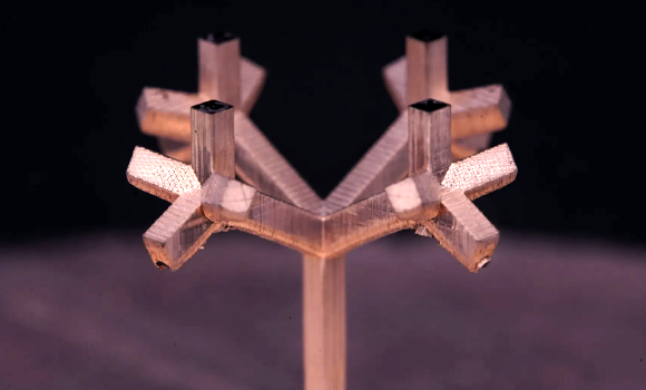
As reported in Nature Communications, the new platform, referred to as charge programmed multi-material Additive Manufacturing (CPD), is a universal system for rapid production of nearly all 3D antenna systems. It can pattern highly conductive metals with a wide range of dielectric materials into a 3D layout.

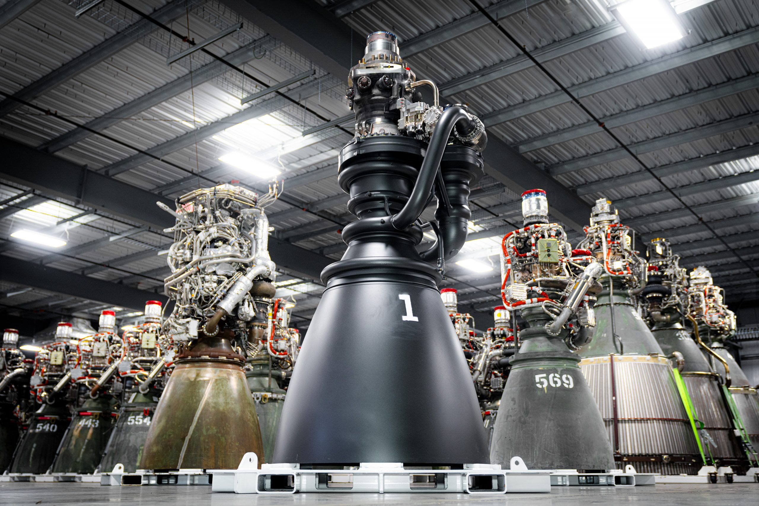
Almost all electronic devices depend on antennas for sending and receiving data. The demand for lightweight antennas is increasing due to new applications such as the latest 5G and 6G networks, advanced wearable devices, and aerospace applications like CubeSats. However, traditional manufacturing techniques have restricted the structural complexity and the use of multiple materials, which could unlock additional features and capabilities for antennas.
Zheng emphasised that the platform is not an expensive Additive Manufacturing machine for metals that would involve pricey metal powders and high-energy lasers, “This technology can be applied to desktop-friendly light-based printers.”
The CPD method combines a desktop digital light Additive Manufacturing machine and a catalyst-based technology that can pattern different polymers at different locations where they will attract metal plating. Its auto-catalytic or selective plating technology enables the polymers to selectively absorb metal ions into prescribed locations that are defined by the desired antenna design outcome.
CPD can broadly integrate with a variety of multi-material Additive Manufacturing methods. Zheng shared, “It allows essentially any complex 3D structure, including complex lattices, and has demonstrated deposition of copper with near pristine conductivity, as well as magnetic materials, semiconductors, nanomaterials and combinations of these.”
Zheng has been working on the CPD platform since 2019, when his group first proposed the concept. In 2020, his team published its first paper in Nature Electronics on this technology, followed by a 2022 paper in Science that described its use to make microrobots.
This latest paper is specific to the antenna application. Zheng stated that CPD is “very uniquely suited for antennas, because nearly all antennas need two components: One is the metal phase, the conductor, and the other is the dielectric phase, which is not conductive — and [until now] there has been no technology capable of directly patterning or synthesizing the conductor and dielectric materials together.”
Zheng explained that the first application they considered was antennas. After discussing the technology with colleagues specialising in this area, they realised that this technique could revolutionise how antennas are additively manufactured and open up new design possibilities.
Manufacturing both the conductor (metal) and dielectric materials is especially important for antennas to be used in extreme environments. Zheng shared, “you cannot use a regular polymer in space. You need a high temperature polymer like Kapton, which is a good material in aerospace [stable at both very high and very low temperatures]. Now you can have Kapton and a pattern of metal traces interwoven in 3D at the same time.”
The team has also shown that through proper 3D designs, these antennas, without having to sit on a bulky substrate, achieve substantial weight savings compared to current antennas.
Co-author Yahya Rahmat-Samii, professor of electrical and computer engineering at UCLA, believes that the CPD platform could significantly expand the possibilities for new antenna technologies and enable data-drive designs – allowing out-of-the box antenna designs for diverse applications. “There are probably numerous different antenna structures, depending on the application you have in mind,” he said.
Zheng and Rahmat-Samii aim to explore the full potential of antenna design using their new Additive Manufacturing technology. By controlling the complexity of an antenna, they can shape electromagnetic waves. To advance applications for this technology, the team at UC Berkeley has established a startup company focused on developing flexible medical sensors that could conform to the shape of a hand.
“We can achieve a tuneable antenna,” Zheng said. “And so the question now is, where can that technology help us best?”