JEOL, NC State and ORNL test PBF-EB tungsten tiles in fusion device
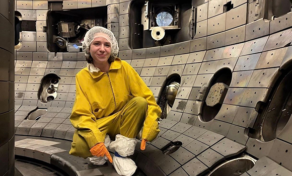
North Carolina State University (NC State); Oak Ridge National Laboratory (ORNL), Tennessee, USA; and JEOL Ltd, headquartered in Akishima, Tokyo, have additively manufactured full-size tungsten tiles for the lower divertor of the DIII-D fusion device. At the DIII-D National Fusion Facility in San Diego, the tile surfaces were exposed to plasma discharges with significant heat and particle flux, and came through intact.
From invitation to installed hardware in approximately eight months, the project was born out of NC State’s research partnership with DIII-D National Fusion Facility, bringing together three groups with expertise in Electron Beam Powder Bed Fusion (PBF-EB) and tungsten Additive Manufacturing. JEOL’s large-format PBF-EB machine, JAM-5200EBM, was used to manufacture the full-size tiles.

“We appreciate the opportunity to collaborate with NC State, ORNL, and General Atomics, on a project that brings together advanced materials research, fusion science, and JEOL’s long-standing expertise in precisely controlled electron beam technologies,” said Tom Isabell, President of JEOL USA. “Producing full-size tungsten tiles for DIII-D is exactly the kind of challenge our JAM-5200EBM system was designed to address. By applying our optics, beam-control, and Additive Manufacturing expertise alongside outstanding partners, we are helping demonstrate a practical path toward the complex, high-performance components future fusion systems will require.”
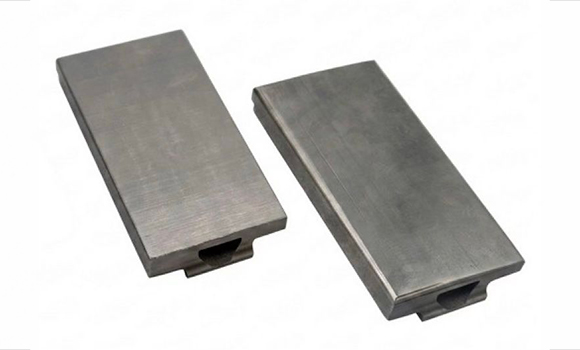
Divertor tiles in ITER and future fusion power plants are expected to withstand steady heat loads of 10–20 MW/m², with brief bursts reaching substantially higher levels, tungsten is considered a leading candidate material, with the highest melting point of any metal, 3,422°C. Each tile pair measures approximately 136 by 143 mm and 20 mm thick.
“Tungsten is currently the material everyone wants in a fusion reactor, but it is extremely difficult to manufacture into complex shapes,” said Dr Michael Kirka, ORNL. “We were able to do this with electron beam Additive Manufacturing, when most of the field thought printed tungsten would always crack. These tiles are the payoff from years of that work.”
Wire Electrical Discharge Machining (EDM) was used to shape the mounting features and a gently domed surface with a radius of about 1 m. A multi-axis CNC grinder, programmed with a digital twin of the tile, then removed about 250 microns from the plasma-facing surface. The tiles were mounted on copper-alloy pedestals and installed in DIII-D’s lower divertor in July 2026. During a three-day testing campaign, they experienced 74 high-confinement plasma discharges at medium-to-high power, totalling approximately four minutes of plasma exposure.
The tiles are now being removed, imaged and surface-scanned to compare with their condition before exposure, prior to returning to NC State for further analysis.
“DIII-D lets us put candidate materials in front of a real fusion plasma and see what happens,” stated Dr Chris Ledford, ORNL. “Seeing additively manufactured tungsten go from small test buttons to full-size tiles in the divertor in less than a year is remarkable, and the data from this campaign will help guide how tungsten components are designed for ITER and beyond.”