

Researchers develop novel method to manufacture plastic-metal composites
Researchers from Waseda University, Japan, and Nanyang Technological University (NTU), Singapore, have developed a new Additive Manufacturing process for the production of metal-plastic composite structures with complex shapes. The details of the multi-material digital light processing AM, referred to in the research as MM-DLP3DP, have been published in ACS Applied Materials & Interfaces.
Metal–plastic composite structures have widespread potential applicability in smart electronics, micro/nanosensing, Internet of Things devices, and quantum computing. Devices constructed using these structures have a higher degree of design freedom and more complex features & geometry at increasingly smaller sizes. Currently, however, producing these composite structures are expensive and complicated.
Explaining the motivation behind the study, lead authors Professor Shinjiro Umezu and Kewei Song from Waseda University and Professor Hirotaka Sato from NTU Singapore stated, “Robots and IoT devices are evolving at a lightning pace. Thus, the technology to manufacture them must evolve as well. Although existing technology can manufacture 3D circuits, stacking flat circuits is still an active area of research. We wanted to address this issue to create highly functional devices to promote the progress and development of human society.”
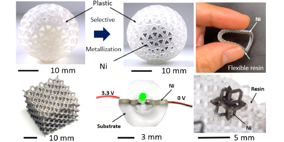
The new paper “New Metal−Plastic Hybrid Additive Manufacturing for Precise Fabrication of Arbitrary Metal Patterns on External and Even Internal Surfaces of 3D Plastic Structures” explains that the new process is multi-step, beginning with the preparation of the active precursors (chemicals which ca be converted in the desired chemical after AM, as these chemicals can’t be additively manufactured alone). Palladium ions are them added to light-cured resins to prepare the active precursors. This is done to promote electroless plating (ELP), a process that describes the auto-catalytic reduction of metal ions in an aqueous solution to form a metal coating. Next, the MM-DLP3DP process apparatus is used to create micro-structures which contain the nested regions of the resin or the active precursor. Finally, these materials are directly plated and 3D metal patterns are added using ELP.
The research team manufactured a variety of parts with complex topologies to demonstrate the manufacturing capabilities of the proposed technique. These parts had complex structures with multi-material nesting layers, including microporous and tiny hollow structures, the smallest of which was 40 μm in size. Moreover, the metal patterns on these parts were very specific and could be precisely controlled. The team also manufactured 3D circuit boards with complex metal topologies, like an LED stereo circuit with nickel and a double-sided 3D circuit with copper.
“Using the MM-DLP3DP process, arbitrarily complex metal–plastic 3D parts having specific metal patterns can be fabricated,” added Umezu, Song, and Sato. “Furthermore, selectively inducing metal deposition using active precursors can provide higher quality metal coatings. Together, these factors can contribute to the development of highly integrated and customisable 3D microelectronics.”
The new manufacturing process is hoped to to be a breakthrough technology for the manufacturing of circuits, with applications in a diverse variety of technologies, including 3D electronics, metamaterials, flexible wearable devices, and metal hollow electrodes.
The paper is available here.