

ORNL develops advanced flaw detection method for Additive Manufacturing
Researchers at the US Department of Energy’s Oak Ridge National Laboratory (ORNL), located in Oak Ridge, Tennessee, USA, have reportedly improved flaw detection in metal parts produced by Laser Beam Powder Bed Fusion (PBF-LB) via a a method that combines post-production inspection of the manufactured part with data gathered from sensors during the build process.
The combined data teaches a machine-learning algorithm to identify flaws in the product. Notably, this approach allows operators to determine the likelihood of accurate flaw detection as reliably as traditional assessment methods, but without the need for excessive time and labour.
“We can detect flaw sizes of about half a millimetre — about the thickness of a business card – 90% of the time,” shared ORNL researcher Luke Scime. “We’re the first to put a number value on the level of confidence possible for in-situ (in-process) flaw detection.”
During manufacturing, engineers know that there will be flaws in the material, but, thus far, many AM processes have not been able to easily detect these flaws. “For regular manufacturing we know what those are and where and how to find them. (Operators) know the probability that they can detect flaws of a certain size, so they know how often to inspect to get a representative sample,” stated ORNL researcher Zackary Snow. “Not having a number makes it hard to qualify and certify parts,” Snow said. “It’s one of the biggest hurdles in Additive Manufacturing.”
“Scalable in situ [sic] non-destructive evaluation of additively manufactured components using process monitoring, sensor fusion, and machine learning” details the process they developed. This process reportedly achieved a 90% detection rate and reduced the likelihood of false positives, thereby preventing the unnecessary discarding of good products.

In the initial research step, aerospace and defence company RTX designed a part similar to one that it already manufactures, providing opportunities to see realistic-looking flaws. RTX then additively manufactured the part multiple times, monitoring the process with a standard near-infrared camera and an additional visible-light camera. Both RTX and ORNL researchers conducted quality inspections afterward using X-ray computed tomography, commonly called CT scans.
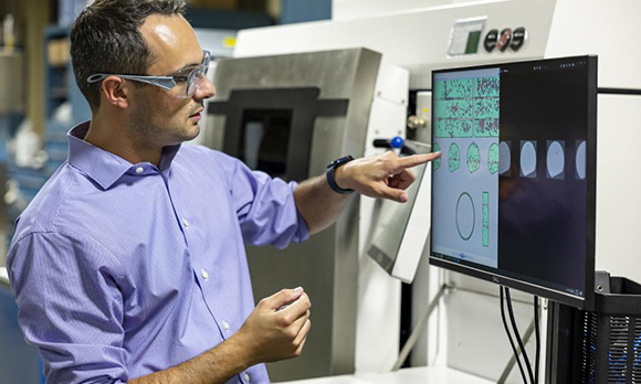
With guidance from RTX, ORNL Additive Manufacturing experts organised the data into a layered stack of images, serving as a guide for the machine-learning algorithm. Initially, the algorithm attempted to label flaws using the CT scan images, with a human operator completing the rest based on visual cues from the manufacturing process data. Continuous human feedback refines the software, enhancing the algorithm’s flaw recognition accuracy each time. ORNL’s previous advancements in in-situ monitoring and deep-learning frameworks played a crucial role in this innovative approach. Over time, this method will minimise the need for human involvement in manufacturing inspection.
Whilst a common method for checking some additively manufactured parts, CT imaging and analysis drives up costs because it requires extra time and expertise. Plus, CT cannot effectively penetrate dense metals, limiting its application.
“This allows CT-level confidence without CT,” Snow said.
When the algorithm is applied to a single design consistently manufactured with the same material and process, it can learn to provide consistent quality analysis within days, said Scime. Simultaneously, the software incorporates all that it learns from different designs and constructions. As a result, it will eventually be capable of accurately checking products with unfamiliar designs.
The ORNL-developed inspection framework could help in expanding Additive Manufacturing applications. With statistically verified quality control, Additive Manufacturing could become viable for mass-producing products like car parts, Snow said.
Diversifying the types of parts that can be additively manufactured is also possible. Knowing the smallest detectable flaw size increases design flexibility. This is crucial as the industry is moving towards larger build volumes and faster build rates. This means more lasers interacting to create larger parts, potentially introducing different types of flaws, according to Brian Fisher, Senior Principal Engineer for Additive Manufacturing at RTX’s Raytheon Technologies Research Center.
“You can really start to save time and money and make a business case when printing larger assemblies – except those are also the hardest to inspect today,” Fisher commented. “The vision is with additive, we can make large, highly-complex parts in very dense materials, which traditionally would be very difficult and expensive to thoroughly inspect.”
Next, the ORNL team intends to train the deep learning algorithm to improve differentiation between types of irregularities and to categorise flaws with multiple causes.
The details of this process have been published in Additive Manufacturing.