

Optomec receives $2 million order for Aerosol Jet electronics AM machines
Optomec Inc, Albuquerque, New Mexico, USA, has announced that one of its existing aerospace and defence electronic systems production customers recently purchased another six Aerosol Jet Additive Manufacturing machines, bringing the customer’s total count to twenty machines. The $2+ million in orders is part of a production ramp plan that is expected to grow to more than thirty systems over the next year.
The customer is said to be a leading global manufacturer with more than $25 billion in annual sales. It has been using Optomec’s patented Aerosol Jet solutions for more than five years. Its latest orders include its first installations of Optomec’s new HD2 machine, which is tailored for inline production in advanced semiconductor packaging and PCB assembly operations. Under the contract, Optomec will also provide Production Recipes for both conductive and insulating materials.
“Optomec is fortunate that many of its customers are at the vanguard in adopting Additive Manufacturing in real-world production applications,” stated David Ramahi, CEO, Optomec. “This particular user is truly a standout in leading the charge when it comes to implementation of 3D Additive Electronics, having shipped 100,000s of products manufactured using Optomec’s Aerosol Jet solution for advanced semiconductor packaging.”
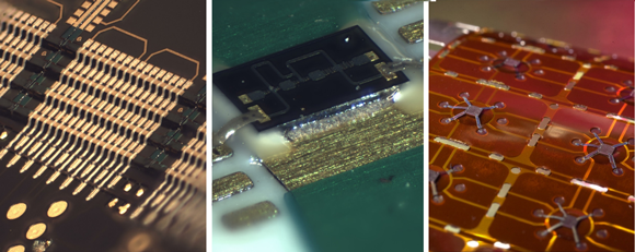
Optomec’s patented Aerosol Jet AM machines are capable of directly building high resolution conductive circuitry, with feature sizes as small as 10 microns. The process is reportedly further differentiated by its ability to build onto non-planar substrates and fully three-dimensional end parts. Production applications include direct building of 3D antennae, 3D sensors, medical electronics, semiconductor packaging and display assembly.
A primary high-value use case in semiconductor packaging is the Additive Manufacturing of 3D interconnects to connect chips to other chips, traditional circuit boards and directly integrated into end-products, such as wearables. In this case, the process replaces legacy wire-bonding due to its advantages in terms of smaller space claim, lower loss (especially in high frequency and mmWave) and greater mechanical reliability.