

New method for Additive Manufacturing metal nanostructures using light

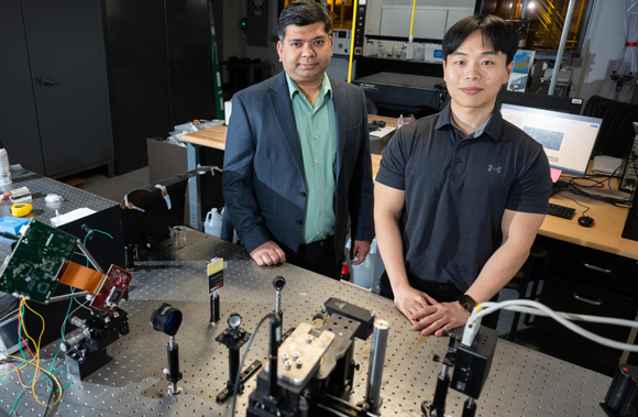
The research article ‘Scalable Printing of Metal Nanostructures through Superluminescent Light Projection’ **by Sourabh Saha, assistant professor in the George W Woodruff School of Mechanical Engineering, and Jungho Choi, a PhD student in Saha’s lab has been published in the journal Advanced Materials.
The article discusses a new method for producing nano-sized metal structures using light, which is reportedly 480 times faster and 35 times cheaper than the current technology. This scalable solution is thought to have the potential to revolutionise the field, which has traditionally relied on technologies that are both expensive and slow.
Manufacturing metal on the nanoscale, a technique known as nanopatterning, is reported to allow for the creation of unique structures with interesting functions. This is critical for the development of various technologies, such as electronic devices, solar energy conversion and sensors. However, it is generally believed that nanoscale Additive Manufacturing required high-intensity light sources or a femtosecond laser, which could cost up to half a million dollars, making it unaffordable for most research labs and small businesses.
“As a scientific community, we don’t have the ability to make enough of these nanomaterials quickly and affordably, and that is why promising technologies often stay limited to the lab and don’t get translated into real-world applications,” Saha stated. “The question we wanted to answer is, ‘Do we really need a high-intensity femtosecond laser to print on the nanoscale?’ Our hypothesis was that we don’t need that light source to get the type of printing we want.”
When looking for an affordable, low-intensity light that could be focused in a way similar to femtosecond lasers researchers turned to superluminescent light emitting diodes (SLEDs) due to their commercial availability. SLEDs reportedly emit light that is a billion times less intense than that of femtosecond lasers.
Saha and Choi embarked on a mission to develop an original projection-style manufacturing technology, designing a system that converts digital images into optical images and displays them on a glass surface. This system works similarly to a digital projector but produces images that are more precisely focused.
The researchers utilised the distinctive characteristics of superluminescent light to produce highly precise images with minimal imperfections. Afterwards, they developed a clear ink solution consisting of metal salt and other chemicals to guarantee that the liquid could effectively absorb light.
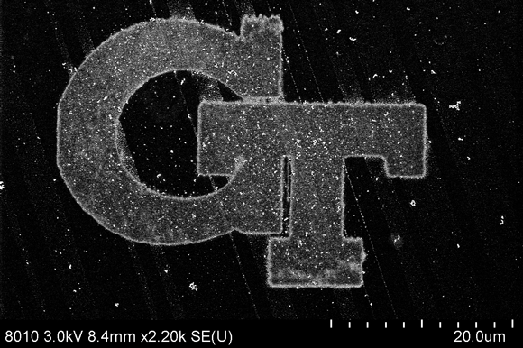
When light from their projection system hit the solution, it caused a chemical reaction that converted the salt solution into metal. The nanoparticles stuck to the glass’ surface, and the agglomeration of the metal particles creates the nanostructures. As the manufacturing process is projection-based, it can construct an entire structure at once, instead of in a point-by-point manner, making it much quicker.
After conducting tests, the researchers found that projection-style nanoscale manufacturing is achievable even with low-intensity light, as long as the projected images are sharply focused. Saha and Choi believe that their work can be easily replicated using commercially available hardware. This would be much more affordable than the femtosecond laser; the type of SLED that Saha and Choi used cost about $3,000.
“At present, only top universities have access to these expensive technologies, and even then, they are located in shared facilities and are not always available,” Choi added. “We want to democratise the capability of nanoscale 3D printing, and we hope our research opens the door for greater access to this type of process at a low cost.”
Saha and Choi believe their technique will be particularly useful for those working in the electronic, optic, and plasmonic fields since these fields require a variety of complex metallic nanostructures.
“I think the metrics of cost and speed have been greatly undervalued in the scientific community that works on fabrication and manufacturing of tiny structures,” Saha said. “In the real world, these metrics are important when it comes to translating discoveries from the lab to industry. Only when we have manufacturing techniques that take these metrics into account will we be able to fully leverage nanotechnology for societal benefit.”
The full article is available here.