

Nikon opens new Nikon Additive Manufacturing Technology Center in Japan
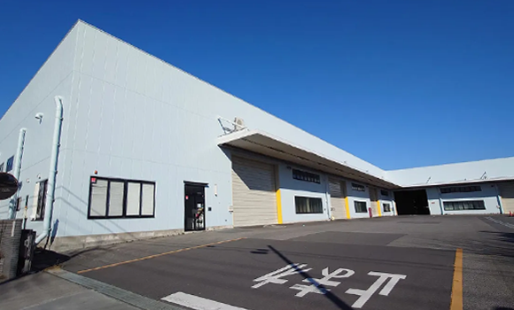
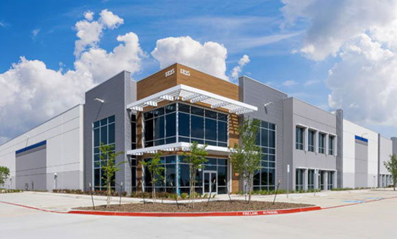
Nikon Corporation, headquartered in Tokyo, Japan, has announced the establishment of its Nikon AM Technology Center Japan, located in Gyoda, Saitama Prefecture. The 922 m2 facility will be unveiled to invited guests at a Grand Opening ceremony on February 28, 2025.
The announcement follows the opening of the first Nikon AM Technology Center in Long Beach, California, USA in July last year.
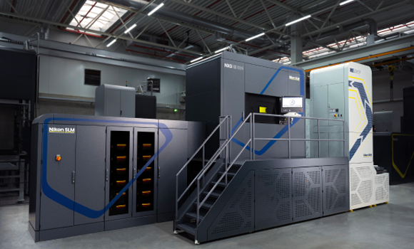
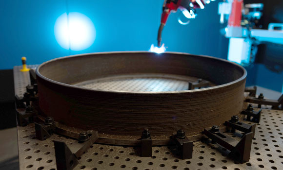
As with the California location, the facility in Japan brings together the Nikon AM portfolio. The centre is similarly equipped with the ultra-large format NXG XII 600 Laser Beam Powder Bed Fusion (PBF-LB) Additive Manufacturing machine from Nikon SLM Solutions AG, reportedly the first of its kind in Japan. The NXG series features twelve lasers with a build platform that, depending on the model, allows printing parts up to a maximum of 1.5 m and will be pivotal in enabling the most demanding AM applications, especially for the defence, space and aviation sectors.

The new facility will also house high-precision Directed Energy Deposition (DED) machines, including the Lasermeister LM300A for repair and maintenance applications across various industries, along with X-ray CT inspection equipment and other key solutions to advance metal AM technology development and processing for customers throughout Japan and Asia.