Georgia Tech adds micro Additive Manufacturing capability with Exaddon CERES
July 26, 2023

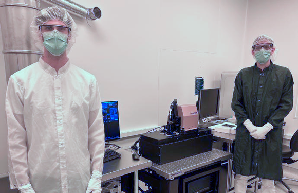
Exaddon AG, headquartered in Glattbrugg, Switzerland, has announced that the Georgia Tech Institute for Electronics and Nanotechnology (IEM), based in Atlanta, Georgia, USA, has purchased a CERES µAM system for use in its Micro/Nano Fabrication Facility. The CERES µAM system operates at room temperature, manufacturing microscale metal structures with <1 µm resolution.
With over 2,800 m2 of clean room space, Georgia Tech reportedly has one of the largest academic nanotechnology research facilities in the Southeastern United States. The facility’s range of microelectronics and nanotechnology equipment includes etching, metrology, thin, films, micromachining, packaging, e-beam lithography, and two-photon lithography.
With CERES, research teams can now additively manufacture pure metal structures directly on pre-patterned chip surfaces in micrometre sizes. Manufacturing with CERES is said to be fully compatible with conventional IC and PCB process steps, allowing for the hybrid manufacture of devices using both µAM and photolithographic processes.
For Exaddon, this is hoped to be a positive step in expanding the presence of µAM within the American academic market, especially given Georgia Tech’s reputation and industry connections. With CERES systems already in use at shared facilities at the University of Oregon and Purdue University, West Lafayette, Indiana, interdisciplinary research teams across the country can utilise the metal µAM technology.
Exaddon CEO Edgar Hepp, shared, “I believe the CERES system acquisition is a fantastic move by Georgia Tech to expand its already impressive array of microelectronic and nanotechnology capabilities, and it underlines its commitment to advancing research in this area.
“With CERES, research teams can take the next step and printing highly conductive metal structures in shapes that are impossible with other technologies. Printing directly on pre-patterned chip surfaces with CERES as part of a process integrated with lithography opens up fantastic research opportunities in semiconductor contacting and repair, MEMS packaging, and more.”
“We look forward to seeing the exciting developments that will doubtless come from this,” Hepp added.
https://research.gatech.edu/nano
Download Metal AM magazine
