Auburn University demonstrates zero-gravity Additive Manufacturing with LASED machine
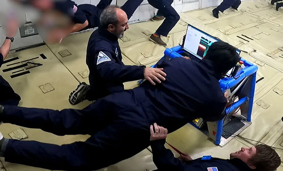
A team of researchers led by Masoud Mahjouri-Samani, the Godbold Associate Professor in the Department of Electrical and Computer Engineering at Auburn University, Alabama, USA, has successfully tested a compact nanoparticle Additive Manufacturing machine aboard a series of NASA-sponsored parabolic flights simulating zero gravity.
The experiment aimed to demonstrate the space functionality of a specially designed Laser Ablation and Sintering Enabled Deposition (LASED) multi-material printer capable of printing various materials, including semiconductors, metals and insulators that can be used to make electronics and semiconductor devices in gravity-challenged environments.
“This was a one-shot win. From the very first parabola, the machine printed beautifully. That level of success on a first flight is extremely rare,” said Mahjouri-Samani, who made the flights with graduate student Aarsh Patel and Colton Bevel, a research engineer at the Auburn University Research and Innovation Campus in Huntsville.
This testing was enabled by an $870,000 grant from NASA, received by the project – In Space Dry Printing Electronics and Semiconductor Devices – earlier this spring.
LASED technology
LASED technology uses in-situ laser ablation to generate pure and dry nanoparticles from solid materials. Next, the nanoparticles are flown out of the build nozzle and laser sintered in real time to additively manufacture various multi-material electronics and semiconductor devices.
“When it comes to space manufacturing, we need sustainable technology that is compatible with the space environment,” said Mahjouri-Samani, founder of NanoPrintek, Inc, an Auburn-based startup that developed LASED. “With printed electronics, the entire industry has been based on wet ink, but ink and liquids are not compatible with space or microgravity environments.
“Our dry LASED multi-material printer also does not require post-processing, a procedure that typically necessitates the use of ovens and/or heaters, which have their own challenges in the space environment. This supply chain-resilient and sustainable technology is an energy-efficient and environmentally friendly process that will open a new realm of manufacturing in space. I am proud that this technology was invented in my lab and doesn’t exist anywhere else worldwide.”
Mahjouri-Samani added, “If we can print better metals, semiconductors, and devices in space, then we might be able to enable new capabilities for terrestrial applications. The space opens up a new realm of manufacturing ecosystem, with, of course, the right technology.”
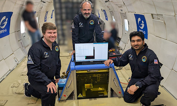
The Additive Manufacturing machine measures 60 cm on each side and consumes less than 500 W, making it well-suited for use aboard the ISS or future lunar missions. Despite its small footprint, the machine includes a fully automated nanoparticle generation system, a delivery mechanism via nozzle, and a sintering process.
“It’s a fully functional machine,” said Mahjouri-Samani. “Everything is integrated. You can programme it to complete complex tasks in twenty seconds. In space, without that time constraint, it can do even more.”
The LASED machine was also engineered to withstand intense conditions.
“We did a lot of simulations and calculations to make sure it could survive take off, landing and the sharp G-force changes,” Mahjouri-Samani said. “Our machine was built to tolerate up to 18Gs – much more than the 2Gs the flight produced. So yes, we were too good.”
Mahjouri-Samani said the device’s plug-and-play performance exceeded even his own expectations. “Other systems sometimes need multiple flights to even get one usable print,” he said. “Ours worked perfectly on parabola one. Once the programmed tests were completed, we had time to print more. We built in a margin for error, but we didn’t need it. We had time left, so we printed extra.”
“We focused on foundational patterns this time,” he continued. “But the real question was: would it print in zero gravity? The answer is yes.”
It was added that there are already plans for a second parabolic test, with a focus on additively manufactured semiconductors. There are also tentative plans to consider sending the AM machine into space for further testing.
www.auburn.edu
www.nanoprintek.com