Fraunhofer ILT to showcase new copper Additive Manufacturing process
August 31, 2017
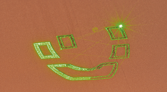
Exposure of a single layer in a SLM process with green laser light to manufacture an internally cooled coil for inductive heat treatment.
The Fraunhofer Institute for Laser Technology ILT in Aachen, Germany, will be presenting a new approach for Selective Laser Melting (SLM) of copper materials at this year’s formnext exhibition in Frankfurt, Germany, November 14–17. The new process, incorporating a green laser, should offer users the first cost-effective AM method for components made of pure and highly conductive copper.
As part of a research project funded by AiF German Federation of Industrial Research Associations, the Fraunhofer ILT researchers are looking to develop the SLM process to make it more suitable for the Additive Manufacturing of components made of copper alloys and pure copper. Pure copper in particular is an attractive option for end users, as it is more electrically and thermally conductive than copper alloys.
“Depending on surface properties, pure copper reflects most of the laser radiation in conventionally used wavelengths of 1 µm,” stated Daniel Heussen, Research Fellow in the Rapid Manufacturing group. As a result, only a small portion of the laser energy is deposited in the material and, thus, is available for the melting process. The reflected radiation can also damage the components of the system. In addition, the absorptivity of the material for the infrared light rises rapidly as the material transitions from a solid to liquid state, thus triggering an unstable and intermittent remelting process.
Using green laser light with a wavelength of 515 nm the absorptivity of pure copper is much higher. This means that less laser power output is needed for a stable process. Furthermore, the laser beam can be focused more precisely, allowing it to manufacture far more delicate components using the new SLM process. A specially developed laser beam source, which operates with green rather than infrared light, will be designed at the Fraunhofer ILT by the end of 2017.
According to Heussen, “We are hoping for a more homogeneous melt pool dynamics so that we can build components with high material density and achieve other positive effects, such as a higher detail resolution.”
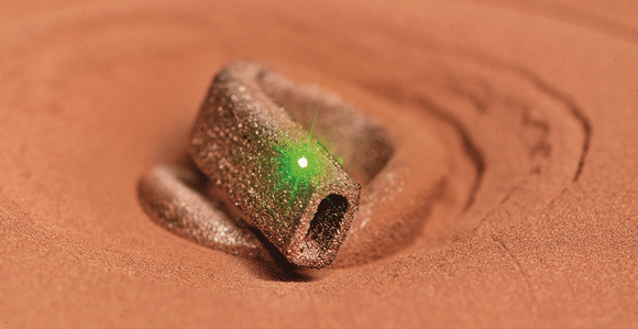
The new process should allow 3D printing of pure copper components
With no green laser source on the market meeting the boundary conditions of the SLM process, the department for laser beam source development at Fraunhofer ILT is building its own in a project they call ‘SLM in green’. The aim is to create a high-quality laser for single-mode operation that functions with a maximum output of 400 watts in continuous service (cw) with green wavelength (515 nm). A ‘SLM in green’ laboratory setup is expected to be ready by the end of 2017. Thereafter, the Fraunhofer ILT will further develop its processes as part of the research project funded by the AiF.
The primary future goal is to create a reliable process with which industrial users can additively manufacture complex geometries of pure copper with hollow structures and undercuts. The process can be used for highly efficient heat exchangers and heat sinks or for the production of delicate, complex electrical components in small batches.
In the field of jewellery design, green laser could offer a far more efficient and reproducible process for manufacturing complex structures than conventional techniques. Compared to other additive methods such as Electron Beam Melting (EBM), the scientists are hoping for a notably higher detail resolution as well as greater cost efficiency in production. The green laser should be suitable not just for copper, but also non-ferrous and precious metals in the jewellery industry. “However, before we achieve that, we still need to overcome a few hurdles in process and system development and gain a deeper process understanding for the use of the new wavelength,” Heussen added. “This is currently the goal of the publicly funded project, which will run until mid-2019.”


